Semiconductor & Scientific Research: Transforming Micro-Designs into Physical Reality
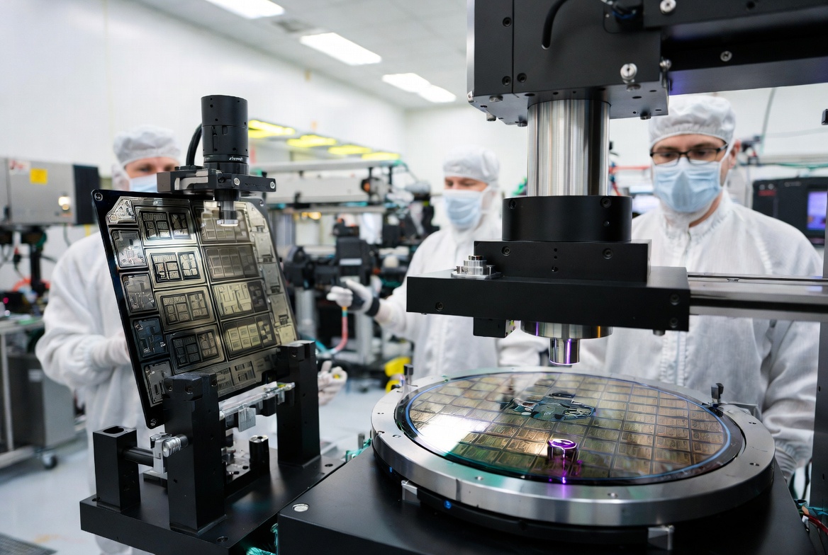
At the bleeding edge of microelectronics and nanotechnology, Photo Reticle provides the essential master photomasks and micro-patterned templates required for advanced manufacturing. Operating at the extreme physical limits of the micro-world, we utilize state-of-the-art direct-write lithography to produce high-resolution masks on chrome-on-glass and quartz substrates, empowering MEMS development, quantum computing research, and IC (Integrated Circuit) prototyping.
The Bridge Between Research and Fabrication
In the semiconductor and scientific sectors, the complexity of a design is often bottlenecked by fabrication capabilities. Photo Reticle serves as the critical bridge from “Digital Design” to “Physical Realization.”
The Foundation of MEMS & Micro-nanofabrication: * Complex Structural Fabrication: Micro-Electro-Mechanical Systems require intricate micro-structures. Our photomasks replicate these designs with sub-micron precision—whether it is the cantilever beam of an accelerometer or the complex channels of a microfluidic chip, our masks provide the perfect physical counterpart.
High Fidelity: We maintain rigorous control over Critical Dimensions (CD) to ensure the absolute fidelity of pattern transfer during the photoresist exposure process. This is paramount for applications like quantum computing chips, where there is zero tolerance for structural defects.
Cleanroom-Grade Quality Assurance:
Defect-Free Manufacturing: Our entire production workflow is conducted within Class 100/1000 cleanrooms, ensuring every mask is free from particulate contamination. In the realm of nanoscale manufacturing, a single speck of dust can lead to the failure of an entire wafer. Our quality control provides a rock-solid guarantee for our clients’ R&D and production cycles.
Core Technical Advantages: Extreme Microscopic Control
Sub-micron CD Control: We possess the capability for extreme control over critical dimensions, meeting the stringent requirements for linewidth uniformity demanded by advanced semiconductor processes.
Rapid Prototyping: Tailored specifically for research institutions and university laboratories, we offer rapid sampling services. This helps researchers verify design concepts in the shortest possible time, accelerating the transition from scientific discovery to market-ready technology.
Diverse Substrate Processing: Beyond standard quartz and chrome-on-glass, we excel in handling specialized substrates, including thin films and various metals, to meet the R&D needs of novel semiconductor materials and optoelectronic devices.
Industry Applications & Value
Integrated Circuits (IC): Prototype verification and small-batch production for ASICs, FPGAs, and other specialized chips.
MEMS Sensors: Fabrication masks for micro-sensors, including accelerometers, gyroscopes, and MEMS microphones.
Frontier Scientific Research: Photolithographic masters for nanostructures like quantum dots, photonic crystals, and superconducting devices.
Compound Semiconductors: Lithography process support for power devices such as GaN (Gallium Nitride) and SiC (Silicon Carbide).