Precision Meets Innovation: How CAD & Nano-Tech are Redefining Reticle Engineering
In the high-stakes world of optoelectronics, precision and innovation aren’t just goals—they are absolute requirements. At Photo Reticle, we remain at the cutting edge of photonics technology, driving the evolution of reticle engineering with a relentless focus on extreme accuracy and cost-effectiveness.
In this deep dive, we explore how modern CAD software and industry-wide advancements are shaping the future of reticle manufacturing and custom optical solutions.
1. Streamlined Manufacturing: Driving Efficiency in Photonics
The production of reticles has undergone a radical transformation. By integrating Computer-Aided Design (CAD) with advanced precision machining, Photo Reticle has significantly accelerated production timelines while increasing total output.
Affordability & Quality: This operational efficiency allows us to offer high-quality, affordable reticles without compromising on the tight tolerances required by high-tech industries.
Market Growth: The precision optics market—where custom reticles play a critical role—is currently valued at $20 billion and is projected to grow by 8% through 2026.
2. Customization and Scalability Through CAD Simulation
One of the most significant barriers in traditional engineering was the prohibitive cost of customization. Today, Photo Reticle utilizes advanced CAD software and digital simulation to shatter that barrier.
Businesses can now order bespoke reticles tailored to their specific technical requirements without the “prototype tax.” This flexibility allows sectors such as medical imaging, aerospace, and robotics to leverage custom photonics technology for specialized applications.
The Power of Digital Prototyping
Minimal Waste: By fine-tuning designs in a digital environment before a single substrate is processed, we minimize material wastage and optimize manufacturing.
Virtual Testing: Our engineers use sophisticated modeling to simulate reticle behavior under various environmental conditions, ensuring every design is “battle-tested” before production.
3. High-Performance, Accessible Materials
A major breakthrough in photonics reticle engineering is the development of cost-effective substrates. While traditional reticles often relied on expensive materials, Photo Reticle offers high-standard alternatives that maintain optical integrity:
Glass Substrates: The gold standard for optical clarity and stability.
Mylar: Ideal for specialized, flexible, and lightweight applications.
Aluminum: Provides exceptional durability and high reflectivity where needed.
4. Unrivaled Accuracy: Nano-Precision Fabrication
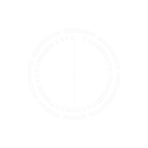
Because reticles consist of microscopic patterns and lines integrated into optical eyepieces, the margin for error is effectively zero. Photo Reticle ensures every measurement is as precise as possible.
Sub-Nanometer Accuracy
The quest for perfection has led to nano-precision fabrication techniques. Utilizing precision-guided technology, we produce patterns with sub-nanometer accuracy—a critical requirement for semiconductor manufacturing and high-end targeting systems.
Advanced Coating Technologies
Accuracy is further enhanced by our specialized coating processes. Our anti-reflective (AR) coatings reduce unwanted glare, significantly improving the signal-to-noise ratio and ensuring your custom reticles maintain their precision over years of use.
The Future: Innovation at Photo Reticle
The pace of innovation in reticle engineering is accelerating. By pooling expertise and embracing the latest advancements in materials and manufacturing, Photo Reticle is proud to provide the precision tools that power tomorrow’s technology.
From aiming and targeting to complex industrial measurement, our reticles are designed to hit the mark every time.