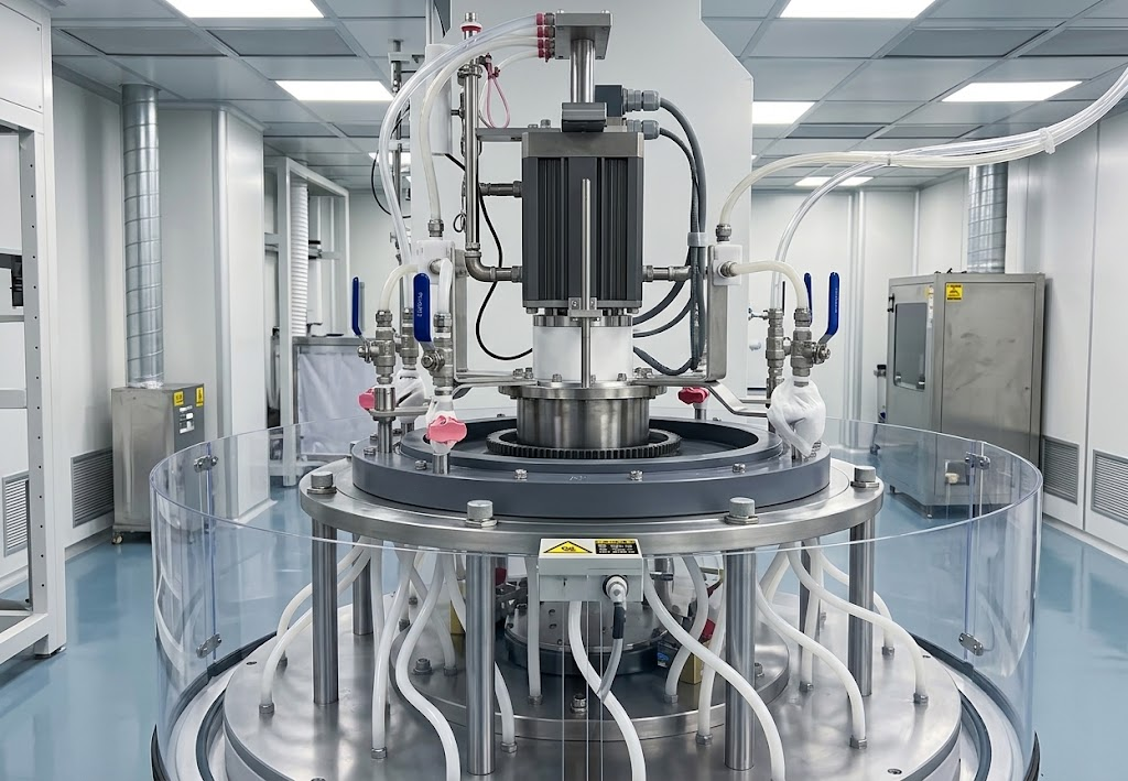
Process glass, fused silica and selected hard substrates with controlled geometry, surface condition, flatness, edge treatment and cleanliness.
Ultra-precision material processing
Flatness control and hard-material processing for precision substrates.
This processing route covers batch and custom work on quartz, ceramics, silicon carbide and carbon materials. The finished process is selected around diameter, flatness, thickness, edge condition and the inspection method required by the component.
300 mm-class flatness and hard-material processing
Our stated capability includes batch-scale processing within a 300 mm diameter field with flatness within 1 µm, and custom processing at the 100 nm flatness level (approximately one sixth of the specified reference wavelength) when the material and measurement plan support it.
Batch processing: flatness within 1 µm over a 300 mm diameter field
Custom process target: 100 nm flatness level over the defined field
Wire cutting, grinding, polishing, laser cutting and laser drilling
Ultra-precision CNC machining with 1 µm positioning accuracy reference
Match the substrate to its optical role
Soda-lime glass is a practical option for many visible-light patterned components. Fused silica is useful when ultraviolet transmission or low thermal expansion matters. Specify the material grade and working wavelength; visual clarity alone does not define spectral performance.
Separate geometry from surface quality
Thickness, total thickness variation, flatness and parallelism describe different aspects of the substrate. Surface scratches and digs describe appearance. Assign each requirement to the useful aperture and the relevant measurement method.
Technical specifications
Precision photomask substrates
Property
Specification
Material
Synthetic fused silica / B270 / soda-lime glass
Square formats
3 / 4 / 6 / 7 / 8 / 9 in
Thickness
≥0.3 mm
Total thickness variation (TTV)
≤2 µm
Flatness
≤2 µm
Encoder glass substrates
Property
Specification
Material
B270 / K9 / soda-lime glass
Maximum diameter
1500 mm
Minimum annular width
5 mm
Thickness
≥0.4 mm
Total thickness variation (TTV)
≤2 µm
Surface figure
λ/4
Concentricity
≤0.02 mm
Special-format glass substrates
Property
Specification
Material
K9 / B270 / soda-lime glass / BF33 / D263T
Maximum diagonal
1500 mm
Thickness
≥0.3 mm
Total thickness variation (TTV)
≤2 µm
Surface figure
λ/2
Polished surfaces are supplied to Grade 0 appearance requirements. Surface-quality grading and the test wavelength for λ-based surface figure are specified on the order drawing.
Choose the substrate for your wavelength and temperature range
Soda-lime glass is a practical starting material for many visible-light masks and patterned components. Low-expansion glass reduces thermal dimensional change. Fused silica is a strong choice when ultraviolet transmission and low thermal expansion are central requirements. Specify the exact glass grade; borosilicate glass and fused silica are not interchangeable names.
Thermal-expansion comparison for substrate selection
Substrate material
Typical linear CTE (×10⁻⁶ K⁻¹)
Fused silica (quartz glass)
0.4–0.5
Low-expansion glass
3.7
Soda-lime glass
9.4
These typical CTE values support material selection. The grade and temperature interval used for a dimensional calculation must be defined on the material specification. A generic low-expansion value does not identify a particular borosilicate grade.
For UV use, specify transmittance at the actual exposure wavelength and substrate thickness. The UV cut-on of soda-lime, white crown and borosilicate glass differs by grade. A thicker substrate can transmit less near its absorption edge; curves measured at different thicknesses are not directly interchangeable.
Small-format substrate flatness options
Choose the format code, glass material and flatness limit together. Each number below is a selectable maximum flatness in micrometres, not a thickness tolerance or a minimum-to-maximum range. These format-based options are separate from the precision-grade specifications above and the coated-blank dimensional schedules.
Flatness by format and glass type
Format code
Fused silica: available flatness limits (µm)
Soda-lime: available flatness limits (µm)
3004
Not listed for this format
5 / 8 / 10
3006
Not listed for this format
5 / 8 / 10
4004
2 / 5 / 6 / 10
5 / 8 / 10
4006
2 / 5 / 6 / 10
5 / 8 / 10
4008
Not listed for this format
5 / 8 / 10
4009
2 / 5 / 6 / 10
5 / 8 / 10
4010
Not listed for this format
5 / 8 / 10
4012
Not listed for this format
5 / 8 / 10
5002
Not listed for this format
8 / 10 / 15
5004
Not listed for this format
8 / 10 / 15
5006
2 / 5 / 6 / 10
8 / 10 / 15
5009
2 / 5 / 6 / 10
8 / 10 / 15
6009
2 / 5 / 6 / 10
10 / 15
6012
2 / 5 / 6 / 10
10 / 15
6023
Not listed for this format
10 / 15
6025
2 / 5 / 6 / 10
10 / 15
7009
Not listed for this format
10 / 15
7010
2 / 5 / 6 / 10
10 / 15
7012
2 / 5 / 6 / 10
10 / 15
Small-format edge and parallelism options
Property
Specification
Edge preparation
Ground edges with a 45° chamfer
Edge squareness: linear deviation / reference length
<0.015 in / 1 in
Face-to-face thickness difference
|A − B| <5 µm
The linear squareness option is separate from the 90° ±5′ blank-edge specification. The A/B requirement compares thickness at two specified locations and does not replace a full-aperture TTV measurement. Identify the selected edge specification, measurement positions, clear aperture and flatness test method on the drawing.
Large-format glass substrates
Large-format substrate flatness is specified by plate dimensions and thickness. Use these limits for the listed large-format configurations rather than applying a small precision-substrate flatness value to every plate size.
Large-format flatness schedule
Thickness (mm)
Plate-dimension range (mm)
Maximum flatness (µm)
3.0 / 4.8
228.6 × 228.6 to 508 × 609.6
≤70
3.0 / 4.8
609.6 × 609.6 to 700 × 800
≤100
7.8
620 × 720 to 700 × 800
≤120
Specify the required plate dimensions within the listed format ranges, the support condition, measurement area and inspection orientation. The supplied specification should identify whether flatness is assessed before or after coating.
Additional substrate defect grades
Select one substrate acceptance profile for the order. The A/C grades below are separate from the small-format blank defect limits and from the A/B/C chromium-pinhole grades. Substrate defects and coating defects are inspected independently.
Grade A / C substrate defect limits
Acceptance grade
Defect type
Defect size, d
Acceptance limit
A
Bubbles
d ≥30 µm
None permitted
A
Bubbles
10 ≤ d <30 µm
≤1
A
Bubbles
d <10 µm
≤3
A
Surface pits
d ≥10 µm
None permitted
A
Inclusions
d ≥10 µm
None permitted
A
Cracks / chips
d >2 mm
None permitted
C
Bubbles
d >50 µm
None permitted
C
Bubbles
10 ≤ d ≤50 µm
≤4
C
Inclusions
d ≥50 µm
None permitted
C
Cracks / chips
d >2 mm
None permitted
Counts refer to defects in the agreed inspection area, not a density per cm². Define the usable area and excluded edges on the drawing. Defect types and size bands not covered by the selected schedule need an explicit acceptance limit.