
Specify the material before the process
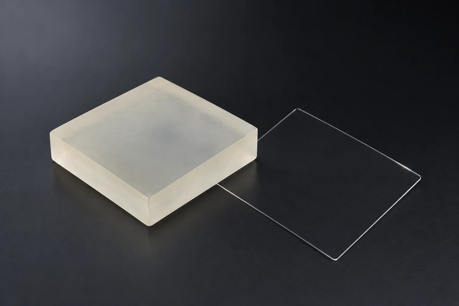
A polished substrate, ready for the next manufacturing step
A fused silica substrate is supplied without chromium, photoresist or a finished pattern. It is the optical and mechanical base for a later coating or lithography process. Specify synthetic fused silica and the required grade; crystalline quartz is a different material, so “quartz” alone is not a complete drawing specification.
Material, geometry and surface condition are separate choices. A plate can have polished faces and still fail a flatness, TTV or parallelism requirement. Define each controlled characteristic independently on the approved drawing.
Geometry and clear aperture
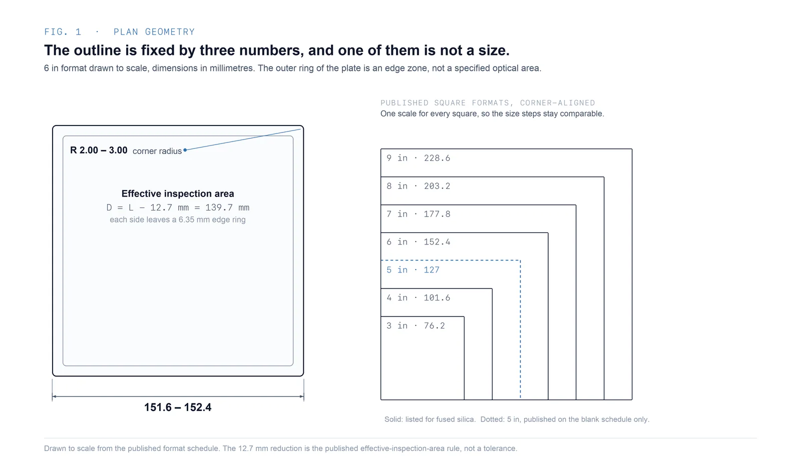
The plate outline and the inspected optical area are not the same thing
State the overall outline, corner and edge treatment, then define the clear aperture separately. Edge zones used for grinding, chamfering, handling or mounting should not be assumed to meet the same optical-area limit unless the drawing says so.
Measurement definitions
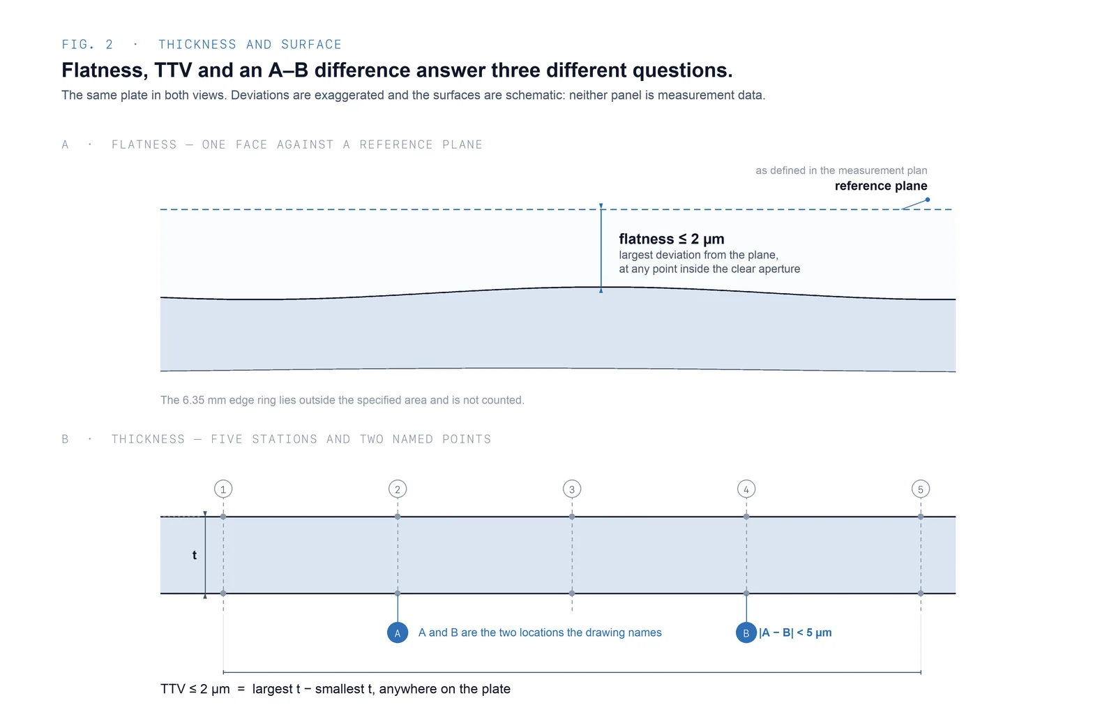
Flatness, TTV and a two-point thickness difference answer different questions
Flatness evaluates one face against a reference plane over a defined aperture. TTV is the maximum measured thickness minus the minimum across the specified area. An A–B value compares thickness at two named positions and does not replace a full-area TTV measurement.
Flatness
Maximum surface departure from the defined reference plane within the stated clear aperture.
Total thickness variation
Largest measured thickness minus the smallest measured thickness over the specified area.
A–B difference
Thickness difference between two dimensioned points chosen for a functional reason such as mounting.
Choose the correct supply stage
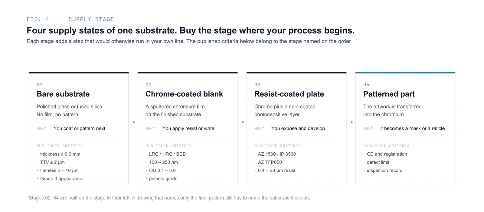
Start with the stage your own process needs
The same substrate can continue into several products. Coating and resist values belong to those later supply stages; they are not default properties of a bare fused silica substrate.
Drawing checklist
Define these items before requesting a quotation
A complete drawing keeps material capability, dimensional inspection and the next process in one specification.
Request a QuoteMaterial and exact fused-silica grade; avoid using “quartz” as the only material description.
Outline or format code, nominal thickness and dimensional tolerances.
TTV limit, flatness limit, measured face, clear aperture and test method.
Edge treatment, corner radius, bevel or chamfer and the mounting exclusion zone.
Surface quality, cleaning state, packaging and required inspection records.
Supply stage: bare substrate, chrome-coated blank, resist-coated plate or finished patterned part.
Acceptance logic
Tie every limit to a location and a measurement method
Final acceptance follows the approved drawing and inspection plan. Values expressed in micrometres and values expressed as a fraction of a wavelength must not be compared until the wavelength, measured face and aperture are defined.
| Outline and thickness | Drawing dimensions, datums and tolerances |
|---|---|
| TTV | Sampling area and maximum-minus-minimum result |
| Flatness | Named face, clear aperture, support condition and test method |
| Surface condition | Agreed defect criteria, cleaning state and excluded edge area |
| Edge | Chamfer or bevel, corner radius and dimensional check |
| Records | Drawing revision and the agreed inspection report |
Related product
Fused Silica Substrates
Review the product configuration, standard specifications and available customization options.