Laser Direct Writing

Heidelberg Instruments laser direct writing for fine chrome patterns, large-area photomasks and aligned mask layers.

Two direct-write routes for fine patterned glass.

The equipment references below show the small-format maskless direct-write route and the Heidelberg DWL 66+ laser writer. Select the writing route around the substrate, field size, minimum feature, overlay requirement and inspection method in the product drawing.

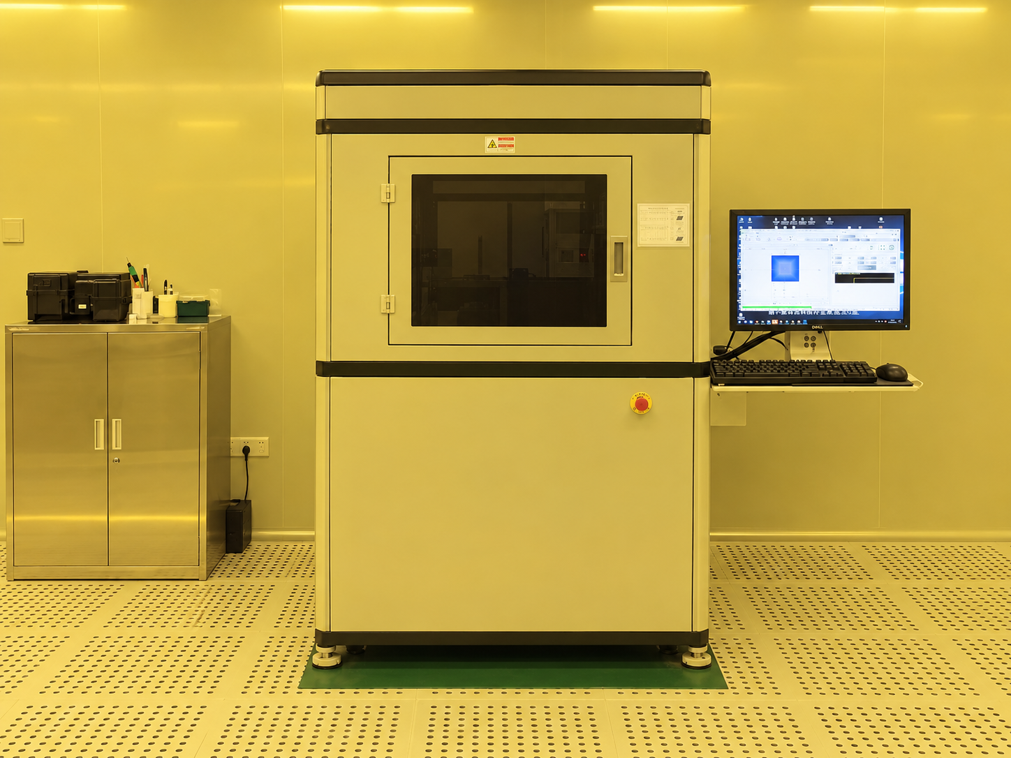
Compact maskless direct-write lithography system in a cleanroom

Maskless direct-write lithography system

A compact precision lithography system for research and production across micro and nano fabrication workflows. It writes directly from digital pattern data, so a separate photomask is not required for each design revision.

  • Minimum line width: ≤600 nm
  • Overlay accuracy: ≤500 nm at 3σ
  • Reference writing speed: 1,000 mm/min
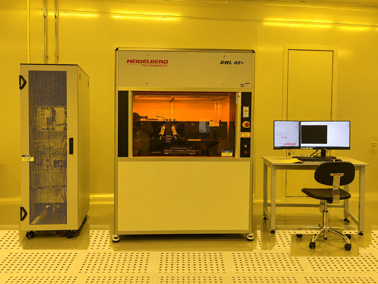
Heidelberg DWL 66+ laser direct-writing system in a cleanroom

Heidelberg DWL 66+ laser direct writing

The Heidelberg route supports fine chrome patterns, larger writing fields, stitching and aligned mask layers. Its equipment values are reference capabilities used during route selection; final product acceptance remains tied to the approved drawing and qualified process.

  • Digital artwork for chromium pattern transfer
  • Writing-mode comparison in the reference table below

Heidelberg laser direct writing for precision photomasks.

The supplied system sheet describes three writing configurations. These values help select a writing mode and set the product drawing; they are not a substitute for a product-specific process qualification.

Heidelberg laser direct-writing reference values
ParameterConfiguration IConfiguration IIConfiguration III
Minimum feature size0.75 µm0.75 µm1 µm
Minimum line and space1.5 µm1.5 µm2 µm
Address grid12.5 nm12.5 nm25 nm
Edge roughness (3σ)30 nm40 nm50 nm
CD uniformity (3σ)55 nm65 nm75 nm
Stitching stability (3σ)30 nm60 nm70 nm
2nd-layer alignment225 nm225 nm350 nm
Write speed485 mm²/min970 mm²/min3150 mm²/min
Exposure time for 100 × 100 mm area28 min14 min5.6 min

System features

  • Light sourceHigh-power DPSS laser, 355 nm
  • Maximum substrate formats9 × 9 in / 17 × 17 in
  • Substrate thickness0–12 mm; other thicknesses on request
  • Maximum exposure fields205 × 205 mm / 410 × 410 mm

How the capability maps to a product

Fine feature size and line/space set the practical pattern limit. Address grid and CD uniformity influence placement and dimensional consistency. Stitching stability matters when the artwork spans more than one writing field. Second-layer alignment is used when a mask set shares alignment marks.

The final mask still depends on resist thickness, exposure dose, development, chrome etch bias, substrate flatness and inspection sampling. Those conditions belong in the product specification and acceptance plan.

Reference conditions355 nm high-power DPSS laser; substrate thickness 0–12 mm; maximum formats and fields depend on the selected configuration and fixture.

Planning your project

Laser direct writing exposes digital artwork in photoresist; development and etching then form the chromium pattern.

Distinguish minimum feature size, address grid, CD uniformity and overlay. Match writing format, substrate and revision-controlled artwork to final inspection.

Does direct writing cut the finished pattern into the glass?

This process describes resist exposure and subsequent film-pattern transfer. Cutting the glass or forming a physical opening is a different operation.

Search