Photolithography

Build fine optical patterns on glass for masks, discs, scales, reticles and custom components.

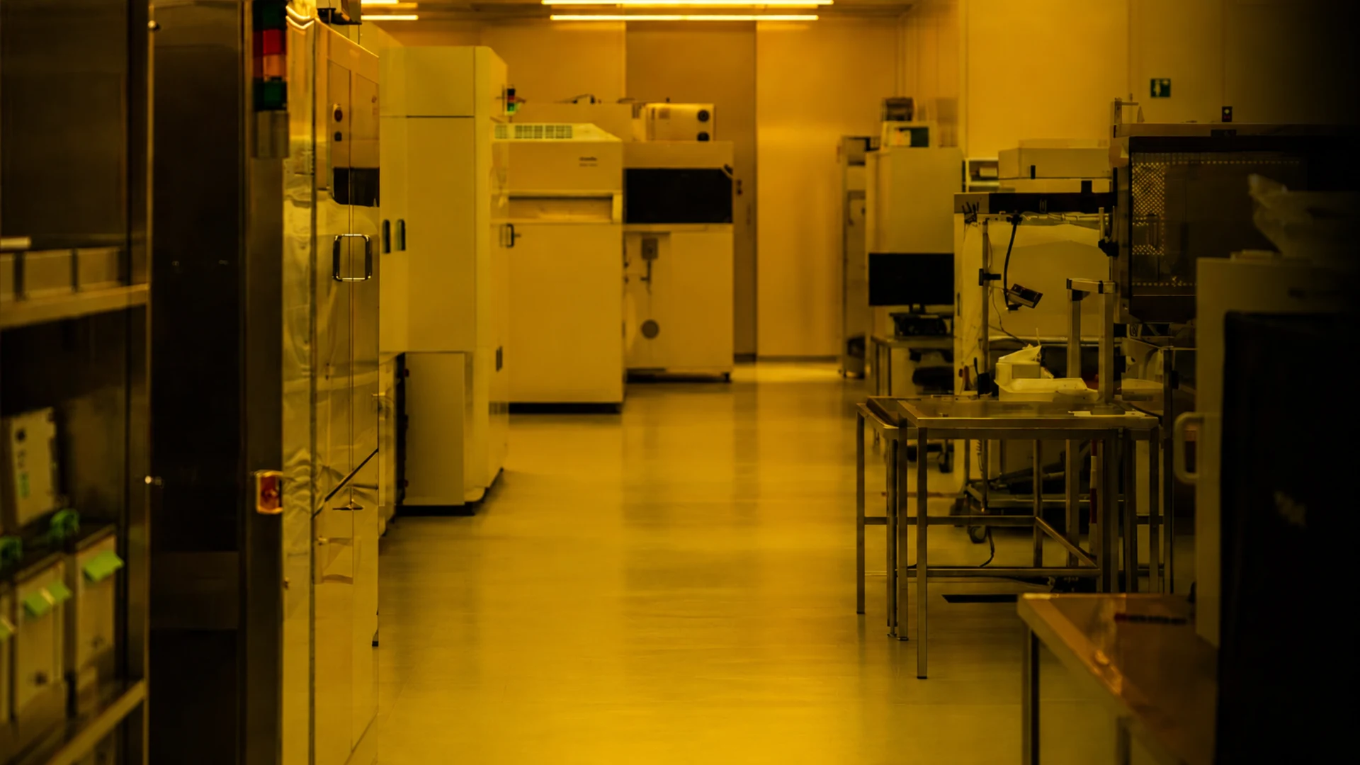
Production equipment on the tloptik manufacturing floor under yellow lighting
Inside our production area

The manufacturing behind the pattern

Glass preparation, coating and patterning take place here. Laser direct writing creates the fine features; inspection checks the finished pattern before it leaves production.

How Chrome-Patterned Glass Components Are Made

A typical manufacturing route for chrome-patterned encoder discs, reticles, scales and targets. The starting material and process steps are selected for each drawing.

  1. 01

    Substrate preparation

    Select, polish and clean the glass to the specified dimensions and surface requirements.

  2. 02

    Chrome sputtering

    Deposit the chromium film with thickness and optical properties defined for the product.

  3. 03

    Photoresist spin coating

    Apply a uniform photoresist layer suited to the patterning process.

  4. 04

    Soft bake

    Bake the coated substrate to remove solvent and prepare the resist for exposure.

  5. 05

    Pattern exposure

    Use laser direct writing or mask exposure according to the product route.

  6. 06

    Development

    Develop the exposed resist to reveal the pattern for subsequent etching.

  7. 07

    Chrome etching

    Etch the exposed chromium to transfer the resist pattern into the film.

  8. 08

    Resist stripping & cleaning

    Remove the remaining resist and clean the patterned surface.

  9. 09

    Final inspection

    Inspect dimensions, pattern features, defects and surface condition against the agreed criteria.

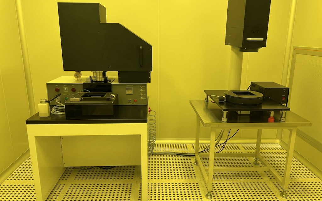
High-precision double-sided replication lithography.

This exposure route is suited to development and production of small and medium-scale integrated circuits, semiconductor devices and surface acoustic wave devices. It combines double-sided alignment with a pneumatic system, vacuum piping and precision mechanics for repeatable exposure handling.

High-precision double-sided replication lithography equipment with an exposure head and alignment stage

What this route supports

  • Suitable for substrates up to 7 inches
  • Supports fragile substrates such as gallium arsenide and indium phosphide
  • Can accommodate non-circular and small-format substrates
  • Pneumatic, vacuum and precision mechanical systems coordinated for exposure

The actual exposure dose, alignment result and repeatability depend on the substrate, resist stack, artwork, fixture and process window agreed for the project.

Planning your project

Photolithography transfers approved artwork into a functional film on a substrate for masks, encoders, reticles and test targets.

The route can include cleaning, coating, resist application, exposure, development, etching, stripping and inspection. Choose the steps for the required supply state.

Can I discuss pattern processing on an already coated substrate?

Provide substrate material, dimensions, film stack, resist state and artwork so the required steps can be matched to the process.

Search