Define the pattern
Set the mark count, diameter, spacing, polarity and finder positions. HALCON create_caltab can generate description and artwork data for the hexagonal plate; verify the output against the production drawing.

Honeycomb circle-grid plates with finder patterns and matching .cpd geometry for HALCON camera calibration.
Discuss your drawingView technical specifications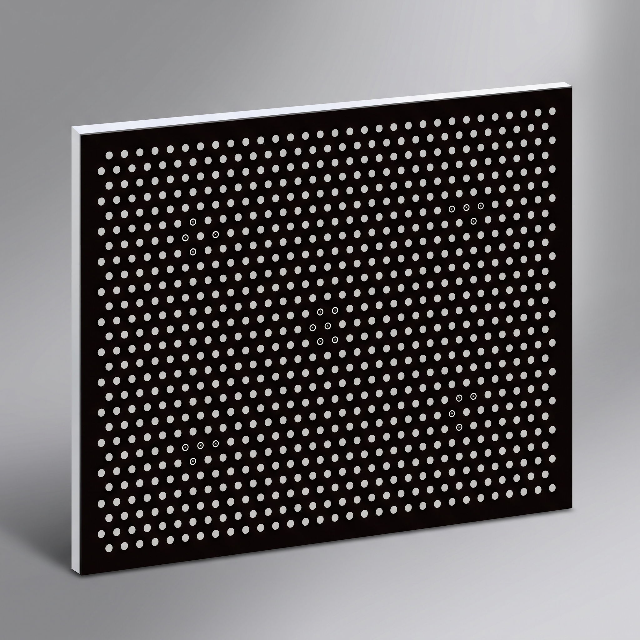
A hexagonal calibration target offsets alternate rows of circular marks. At equal nearest-neighbour pitch, each interior mark has six neighbours and the pattern can carry more points per area than a square grid. This changes the sampling geometry; it does not by itself guarantee a better calibration.
The finished plate, its coordinate model and the detector must describe the same rows, point order and finder positions.
Select a layout to see how neighbouring rows change. This is a geometry comparison, not a claim that one layout always measures better.
Adjacent rows are offset. Each interior point has six nearest neighbours at the defined pitch.
Rows align. Each interior point has four nearest neighbours along the two grid axes.
A repeating dot lattice does not identify which point is which. Selected groups of ring-like, hole-marked dots break that symmetry, allowing HALCON to identify the plate orientation and assign detected centres to the coordinate model.
Each finder group is defined around a central mark and six neighbours, with selected marks carrying holes. At least one complete group must remain in the image. Group positions and hole assignments must match the artwork and .cpd description; partial or blurred groups can prevent reliable detection.
The description file supplies the real mark coordinates and finder geometry used by the calibration model. A file from another drawing revision can yield a plausible fit while giving the wrong physical scale.
| Standard square grid | gen_caltab / .descr |
|---|---|
| Hexagonal circle grid | create_caltab / .cpd |
| Mark arrangement | Hexagonal lattice with alternating rows offset by half the horizontal pitch |
|---|---|
| Mark geometry | Diameter, horizontal pitch, row spacing, count and physical centre coordinates |
| Finder patterns | Hole-marked groups at drawing-defined positions; at least one complete group must be visible to the detector |
| Polarity and illumination | Light marks on a dark field or dark marks on a light field, matched to the detector and substrate |
| Description data | The .cpd calibration-plate description must match the manufactured geometry and revision |
Set the mark count, diameter, spacing, polarity and finder positions. HALCON create_caltab can generate description and artwork data for the hexagonal plate; verify the output against the production drawing.
Keep marks and at least one complete finder pattern sharp and visible while covering the image centre, edges and useful tilt angles.
Set the camera and calibration-object models, collect observations with find_calib_object, then run calibrate_cameras. Review the overall reprojection error and validate the result independently.
The glass, ceramic and film values below describe distinct material and process options. Select a combination through the approved drawing; the geometric pattern and its .cpd data must then match the finished plate.
Fused silica or soda-lime glass with a photolithographic dot pattern.
| Substrate | Fused silica / soda-lime glass |
|---|---|
| Process | Photolithography |
| Line-width tolerance | ±0.2 µm |
| Minimum feature width | 0.55 µm or 1 µm, by pattern configuration |
| Feature and overall accuracy | ±1 µm |
| Clear-area transmission | >95% at 550 nm |
| Chrome finish | Yellow, low-reflection blue or bright chrome |
| Optical density | Yellow chrome OD 3; blue chrome OD 5 |
| Glass thickness | 1, 1.6, 2.3 or 3 mm (±0.2 mm) |
| Large-format glass thickness | 4.8 mm for the 500 × 500 mm format |
| Outline size | From 2 × 2 mm up to 800 × 960 mm |
| Outline tolerance at maximum format | ±0.1 mm at 800 × 960 mm |
| Fused-silica expansion | <5.0 × 10⁻⁷/K at 20–200°C |
| Low-reflection chrome reflectance | <13.4% at 550 nm; <1.8% at 650 nm; <2.67% at 750 nm |
| Surface flatness | <0.55 µm for lengths <50 mm; <2 µm for lengths <100 mm; <5 µm for lengths >100 mm |
| Chrome coating thickness | 120 ±5 nm (1200 ±50 Å) |
| Surface roughness | <0.025 µm |
| Optional white backing | 40 µm coating; 10 µm minimum feature width |
| Outline shape | Square |
| Pattern polarity | Opaque dots or clear dots |
Opaque ceramic plates with matte or bright chrome patterns for reflective imaging.
Opaque ceramic is used with reflected light; it cannot form a backlit clear-dot plate.
| Substrate | Zirconia or alumina ceramic |
|---|---|
| Process | Photolithography |
| Line-width tolerance | ±0.2 µm |
| Pattern options | Matte chrome on matte ceramic; bright chrome on glossy ceramic |
| Minimum feature width | 4 µm matte; 2 µm glossy |
| Feature accuracy | ±2 µm |
| Outline accuracy | ±0.05 mm |
| Ceramic thickness | 1 mm (±0.1 mm), 2 mm or 3 mm (±0.1 mm) |
| Outline size | From 2 × 2 mm up to 228 × 228 mm |
| Outline size tolerance | ±0.1 mm at minimum and maximum formats |
| Flatness | <30 µm below 100 mm; <60 µm below 200 mm |
| Chrome coating | Matte chrome or bright chrome |
| Chrome thickness | 120 ±5 nm (1200 ±50 Å) |
| Surface roughness | 0.2–0.7 µm |
| Thermal expansion | <6.7 × 10⁻⁶/K at 40–400°C |
| Matte chrome reflectance | <12.88% at 550 nm; <10.62% at 650 nm; <12.23% at 750 nm |
| Bright chrome reflectance | <9.56% at 550 nm; <1.89% at 650 nm; <11.168% at 750 nm |
| Density | ≥3.66 g/cm³ |
| Rockwell hardness | ≥80 HRA |
| Optional protection | Thin protective layer above the chrome pattern |
| Edge and hole options | Laser-cut outline, hole, chamfer or bevel |
| Pattern polarity | Opaque pattern or clear pattern |
| Finish and shape | Matte or glossy; square, elliptical or drawing-defined cutouts |
A thin, lightweight format for larger patterns where mounting and ambient conditions are controlled.
| Process | Photographic-film lithography |
|---|---|
| Application | Transmitted-light or backlit functional testing |
| Minimum feature width | 10 or 30 µm |
| Feature accuracy | ±10 µm |
| Film thickness | 0.18 mm (±0.01 mm) |
| Temperature-related dimensional change | 10 µm per °C per metre |
| Environmental response | Film dimensions also respond to humidity; control temperature and relative humidity during coordinate measurement |
| Emulsion | Silver halide, approximately 2 µm |
| Clear-area transmission | >90% across 400–700 nm |
| Optical density | OD >4 in solid black; grayscale density can be specified |
| Maximum format | 0.71 × 0.81 m at 10 µm minimum width; 1.68 × 3.5 m at 30 µm |
| Maximum-format tolerance | ±0.1 mm for both maximum formats |
| Pattern and cutting | Black, grayscale or sinusoidal grayscale; straight, laser-cut or perforated outline |
Camera and lens calibrationKnown mark coordinates support estimation of camera parameters and lens distortion from multiple views.
Stereo and multi-camera systemsObservations in each camera support estimation of relative pose when the chosen calibration model and capture geometry are suitable.
Machine vision measurementA calibrated camera model supports geometric correction and measurements on a defined working plane or with an additional depth constraint.
Robot guidanceCombine plate observations with robot poses in a separate hand-eye calibration workflow.
It is a circle-grid plate whose alternating rows form a hexagonal lattice. The physical point coordinates, finder patterns and description data together define the calibration object.
No. The hexagonal lattice can place more points in an equal-pitch area, but accuracy depends on target geometry, imaging, detection, camera model and independent validation.
A regular lattice repeats under rotation. Distinctive hole-marked groups let the detector establish plate orientation and point order; their geometry must match the .cpd file.
No. Standard square-grid and create_caltab hexagonal plates use different description formats. Use the file generated for the actual plate and HALCON workflow.
No. Its Error output is the overall back-projection RMSE. Inspect stored observations and residuals separately when investigating individual views.
Glass or film can carry clear marks in an opaque coating. Opaque ceramic is intended for reflected-light arrangements and cannot form transmissive holes simply by opening the chrome layer.
Send the drawing, working field, HALCON version, lighting mode and required description-file format so the physical plate and software model can be checked together.
Request a quoteHALCON hexagonal calibration targets arrange circle centres on an alternating-offset hexagonal lattice, with finder features at defined locations.
Use the matching create_caltab geometry and .cpd calibration-object data. Preserve the required finder pattern, pitch, diameter and arrangement when scaling or modifying artwork.
HALCON version, hexagonal geometry, dot diameter and pitch, finder arrangement, .cpd data, substrate and active field.
No. It describes the arrangement of circle centres. A transparent or dark film feature is distinct from a mechanical through-hole.