
Contact and proximity photomasks: the gap budget and the chrome-side decision
Two choices fix what your mask can print — how far the chrome sits from the resist, and which face of the plate carries it. Both are usually settled by accident, months before anyone measures a printed feature.
The short answer
In contact exposure the printed edge is limited by the plate. In proximity exposure it is limited by the gap: the transition at the printed edge widens as 0.83√(λg), and a feature needs roughly twice that edge width to survive. At 365 nm, a 25 µm gap supports about 6 µm features — not 1 µm.
If the chrome faces away from the resist, the glass thickness joins the light path. 2.3 mm of soda-lime is 1.51 mm of air, which moves the same limit to about 47 µm. This is not a small preference; it is a factor of eight in feature size.
Two words, three distances
A contact photomask is a plate whose patterned face is meant to touch the photoresist. A proximity photomask is the same plate held at a defined distance from it. The artwork, the chrome and the substrate route are identical; what differs is a single length, and everything downstream of it.
That length is where most of the confusion starts, because "the gap" is used for three different quantities.
| Quantity | What it is | Who controls it |
|---|---|---|
| Mechanical gap g | The physical clearance between the chrome surface and the resist surface. Hard contact is about zero; soft contact leaves a few micrometres; proximity is whatever the tool sets. | Your aligner and its fixture |
| Glass path t ÷ n | The air-equivalent distance light travels inside the plate, for paraxial propagation. A 2.3 mm soda-lime plate at n = 1.52 equals 1.51 mm of air. | The plate thickness you order |
| Effective gap | The distance the diffracted light actually propagates after the pattern: g when the chrome faces the resist, g + t ÷ n when it faces away. | The chrome-side decision on the drawing |
Only the effective gap sets the printed edge. The first two are inputs to it.
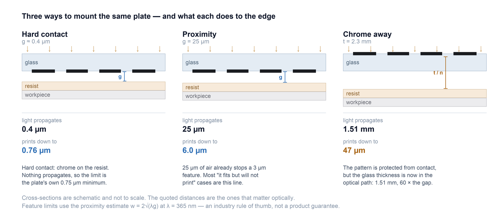
Two practical points follow. First, "contact" is rarely exactly zero: soft contact and vacuum contact both leave a residual gap, and that residual belongs in your calculation rather than in a footnote. Second, a proximity mask does not become a contact mask by being pushed closer at the fixture — the gap has to be specified, held, and stated on the drawing, because the mask is reviewed against it.
What the gap does to the printed edge
Diffraction at the edge of an opaque chrome feature spreads the light that defines it. For a straight edge at a distance g, the transition from dark to bright is not a step but a slope, and the width of that slope — measured between 10% and 90% of the open-field intensity — grows with the square root of the gap.
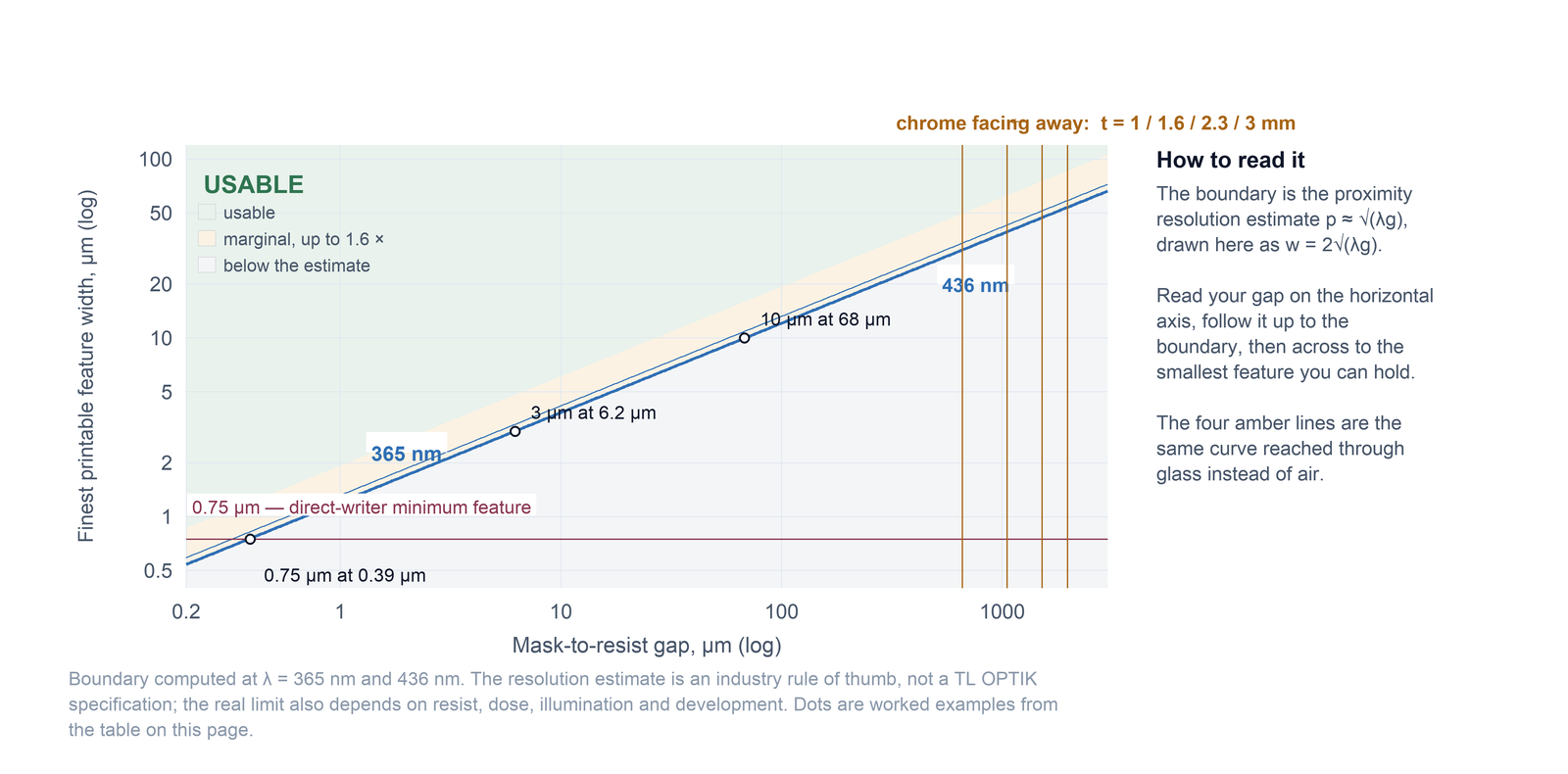
For a coherent edge the exact Fresnel solution gives a transition width of B = 0.83√(λg). The familiar proximity-printing resolution rule, that a half-pitch needs about √(λg), is the same statement with a factor on it: a feature needs roughly 2.4 × B of edge width to keep usable contrast, and 2.4 × 0.83 ≈ 2. So the smallest printable feature width is about 2√(λg), and it is the same relation read the other way.
| Gap g | Edge width B | Smallest feature 2√(λg) | What this rules out |
|---|---|---|---|
| 0.4 µm | 0.32 µm | 0.76 µm | Nothing the writer can produce — the plate becomes the limit |
| 1 µm | 0.50 µm | 1.21 µm | 1 µm lines and spaces |
| 2 µm | 0.71 µm | 1.71 µm | Thin-resist sub-2 µm work |
| 5 µm | 1.12 µm | 2.70 µm | Most 2–3 µm circuit artwork |
| 10 µm | 1.58 µm | 3.82 µm | 4 µm features at the edge of the field |
| 25 µm | 2.50 µm | 6.04 µm | Everything below about 6 µm |
| 50 µm | 3.53 µm | 8.54 µm | Display and PCB artwork below 9 µm |
| 100 µm | 5.00 µm | 12.1 µm | Coarse work only |
B = 0.83√(λg) is computed from the Fresnel edge solution. The feature column is the industry proximity estimate p ≈ √(λg) for half-pitch, doubled. Both are optical arithmetic, not measurements of a printed wafer, and neither is a TL OPTIK specification.
Row five is the one that surprises people. A 10 µm gap sounds like contact with a hair's clearance, and it already costs 3.8 µm of feature size. This is why a mask can pass every dimensional check on the plate and still fail to print: the plate was never the problem.
Turn it round: how much gap your smallest feature allows
At quotation time the question arrives the other way. You know the smallest feature on the artwork and the gap your tool holds. Solving 2√(λg) for g gives the gap you can afford:
| Smallest feature on the artwork | Maximum gap | At 436 nm | Practical reading |
|---|---|---|---|
| 0.75 µm | 0.39 µm | 0.32 µm | True contact only — and the writer's own limit |
| 1 µm | 0.68 µm | 0.57 µm | Hard contact, no residual gap |
| 1.5 µm | 1.5 µm | 1.3 µm | Hard contact with a tight fixture |
| 2 µm | 2.7 µm | 2.3 µm | Soft contact, gap measured |
| 3 µm | 6.2 µm | 5.2 µm | Soft contact or a very tight proximity tool |
| 5 µm | 17 µm | 14 µm | Ordinary proximity |
| 10 µm | 68 µm | 57 µm | Comfortable proximity |
| 20 µm | 274 µm | 229 µm | Thick plates, loose fixtures |
Maximum gap = (w ÷ 2)² ÷ λ. The 436 nm column shows what a longer exposure wavelength costs: for the same feature size, 16% less gap is available.
Three worked cases
4 µm features on a tool that holds a 15 µm gap. The boundary at 15 µm is 4.7 µm, so the 4 µm detail is already below it. Closing the gap to about 11 µm brings the boundary down to 4.0 µm. If the fixture cannot hold 11 µm, the artwork has to be redrawn for a larger minimum feature — no amount of mask precision recovers it.
10 µm features at an 80 µm gap. The boundary at 80 µm is 10.8 µm, which is 8% too coarse. Reducing the gap to 68 µm, or accepting 11 µm features, both solve it. Which one is cheaper depends on the fixture, not on the plate.
2 µm features at any proximity gap. The boundary at 5 µm is already 2.7 µm. There is no useful proximity setting for this artwork; it needs contact, and the contact has to be real. This is the case where ordering a "proximity mask with a small gap" quietly fails.
The chrome-side decision
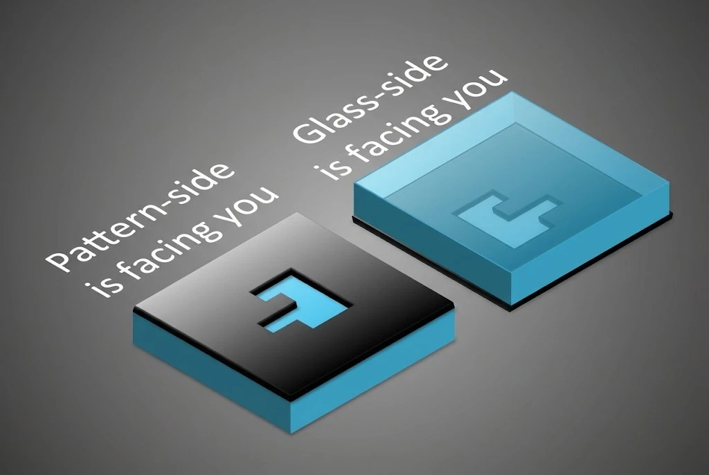
Which face carries the chrome is usually decided once, early, by whoever drew the first version of the part — often to protect the pattern from being touched. The protection is real. So is the cost.
When the chrome faces the resist, the light is diffracted at the pattern and propagates through the gap. When the chrome faces away, the light is diffracted at the pattern and then propagates through the full glass thickness before it ever reaches the air gap. Thickness stops being a mechanical property and becomes an optical one.
| Plate thickness | Glass path t ÷ n | Versus a 25 µm gap | Smallest feature | Where it still works |
|---|---|---|---|---|
| 1.0 mm | 658 µm | 26 × | 31 µm | Large apertures, windows, coarse marks |
| 1.6 mm | 1,053 µm | 42 × | 39 µm | Coarse patterns only |
| 2.3 mm | 1,513 µm | 60 × | 47 µm | Not for lithography at these dimensions |
| 3.0 mm | 1,974 µm | 79 × | 54 µm | Structural plates with coarse artwork |
Thickness options are those published for TL OPTIK chrome-on-glass plates (1, 1.6, 2.3 and 3 mm, ±0.2 mm). n = 1.52 is a typical value for soda-lime at visible and near-UV wavelengths; take n for your own glass grade. Feature values are the same 2√(λg) estimate at λ = 365 nm.
So there is a defensible reason to put the chrome away from the resist, and it is not optical: the pattern never touches anything, so it cannot be worn, contaminated by resist, or scratched by the workpiece. If your smallest feature is comfortably above 50 µm, that trade is free. Below it, the trade is not a trade at all — the geometry simply does not close.
Two further consequences are worth stating because they are easy to miss. In the chrome-away configuration, the plate's internal quality — bubbles, inclusions, polishing marks, striae — sits inside the imaging path, where in the chrome-toward-resist configuration it only sits in the illumination. And the plate's total thickness variation, published at ≤2 µm for TL OPTIK photomask substrates, is 0.1% of a 1.5 mm optical path, so it does not matter in that configuration but does matter in the other one.
Where this page stops. The gap, the illumination and the resist belong to your exposure tool. TL OPTIK supplies the plate and reviews the artwork against the conditions you state. We do not measure your gap, we do not certify a printed dimension, and a plate that satisfies every value on its drawing can still print outside tolerance if the process conditions differ from those the pattern was reviewed for.
What else the gap changes
Two different failures get filed under "the gap was wrong", and they need different fixes.
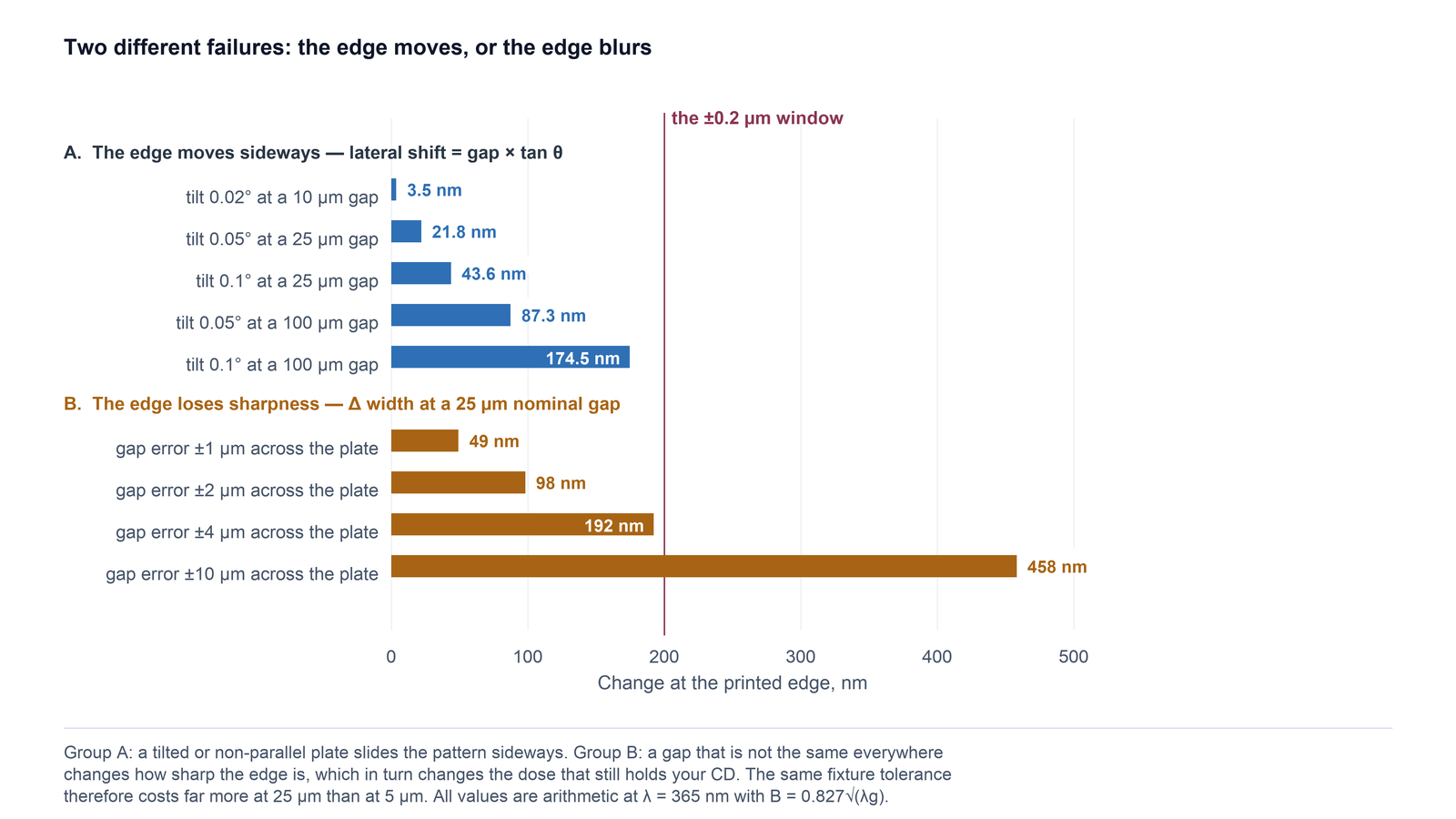
The edge moves. A plate that is not parallel to the workpiece, or a workpiece that is tilted in its holder, shifts the pattern laterally by g × tan θ. The shift grows with the gap, so a tolerance that is harmless in contact becomes significant in proximity: 0.05° at a 25 µm gap is 22 nm, and the same tilt at 100 µm is 87 nm — a large fraction of a ±0.2 µm window.
The edge softens. A gap that is not the same everywhere changes how sharp the edge is, and therefore which dose still lands your critical dimension. Because B scales as √g, the sensitivity is worst at small gaps: at a 25 µm nominal, a ±2 µm variation across the plate changes the edge width by 98 nm, and a ±4 µm variation by 192 nm — comparable to the whole CD window, from flatness alone.
Two more contributors are usually overestimated and one is usually underestimated. A particle trapped under a contact mask lifts the plate locally, but the optical effect is modest: a 10 µm particle creates a 10 µm local gap, which is still far below the feature sizes a contact process is used for. Its mechanical effect — a scratch, a resist smear, a permanent defect — is the real problem, and it is an inspection question, not an optical one. What is usually underestimated is the resist itself: TL OPTIK plates are coated between 0.4 µm and 20 µm depending on the resist family, and that thickness sets the swing curve and the dose latitude long before the gap does.
Contact wears the plate
Contact exposure puts the patterned chrome against a resist-coated workpiece on every shot. Whatever is on either surface is now between them. The consequences are cumulative and they are not a defect of the mask; they are a property of the mode.
Three things make the difference between a mask that lasts and one that does not, and all three belong in the order rather than in a later complaint:
- Which contact. Hard contact, soft contact and vacuum contact load the pattern very differently. State which one the plate is designed for.
- The cleaning and re-qualification plan. A plate that will be cleaned between runs needs its defect limits and its inspection method agreed for the cleaned state, not only for the as-delivered state.
- Whether it is a working plate or a master. If the plate will be consumed, say so; if it must survive, the process must be designed around that, possibly by exposing from a working copy.
Localised chromium repair is available and is genuinely useful for isolated opaque or clear defects found at incoming inspection. It is a corrective operation on a small area, not a way to extend the life of a worn pattern: once the defect density or the registration has moved, repair is not the answer and a new plate is.
What can be verified on the mask, and what only appears on the wafer
This is the part of the conversation that most often goes wrong, and it is a matter of separating two lists rather than of trusting anyone more.
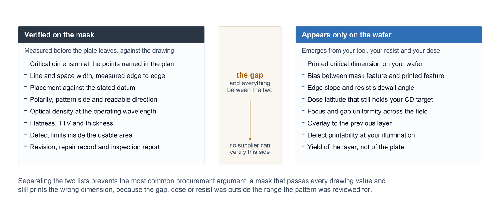
The published line-width tolerance for a finished TL OPTIK mask is ±0.2 µm. That number describes a measurement on the plate, at the points and with the method named in the inspection plan. It does not describe a printed feature, because the printed feature also contains the gap, the dose, the resist, the development and the etch.
So acceptance is agreed in two layers. The plate is accepted against its drawing: critical dimension at stated points, line and space width, placement against the datum, polarity and viewing direction, optical density at the operating wavelength, flatness and thickness, and the defect limits inside the usable area. The layer is accepted against your process, using a witness or a test exposure that you control. Asking a mask supplier to guarantee the second layer is asking for a number nobody can measure at the point of shipment.
What to put in the request
The drawing carries the plate. A short process note carries the reason the plate will work. Both are needed for a quotation that means anything.
On the drawing
- Artwork file and revision, in DXF, GDSII or Gerber
- Clear and opaque polarity, stated explicitly rather than as "positive"
- Pattern side, viewing direction, and whether text must read correctly or mirrored
- Critical dimensions and the points where they are measured
- Minimum line width and minimum space, separately
- Placement datum and alignment marks
- Usable area, edge exclusion and outline dimensions, as separate values
- Substrate material, thickness, flatness and TTV
- Optical density or reflectivity at the operating wavelength
- Defect limits inside the usable area, and the inspection record required
In the process note
- Exposure mode: contact, soft contact or proximity
- Nominal gap and the tolerance the fixture actually holds
- Exposure wavelength, and whether the source is filtered or broadband
- Illumination geometry, if it is unusual
- Resist family and coated thickness
- Workpiece material, size and flatness
- Whether the plate will touch the resist, and how often
- Cleaning method between uses, if the plate is reused
- Quantity, and whether a first article is required
If a value is not yet fixed, say so and give the range under consideration. A gap stated as "10–30 µm, not yet measured" is more useful than a single number that turns out to be aspirational, because the artwork can be reviewed against the worst case in the range.
Common questions
Can a proximity mask print 1 µm features?
Not at any gap a production aligner holds. At 365 nm the estimate gives 2√(λg); a 1 µm gap already supports only 1.2 µm, and a 25 µm gap supports 6 µm. Features near 1 µm require contact exposure with a genuinely small residual gap, or a different imaging route altogether.
Which face should carry the chrome?
Toward the resist, unless there is a specific reason not to. When the chrome faces the resist, the only distance light propagates is the gap. When it faces away, the glass thickness joins the path and the effective gap becomes millimetres. The exception is coarse artwork where the pattern must be protected from contact — above roughly 50 µm feature size, the trade costs nothing.
What gap should I specify on the order?
The one your fixture actually holds, with its tolerance, not the one you would like. Both values are process inputs: we review the artwork against them and will say when the minimum feature cannot survive the gap. We cannot confirm or adjust the gap on your tool.
Does a thicker plate make proximity printing worse?
Only if the chrome faces away from the resist. In that configuration the effective gap includes the glass path, so 3 mm instead of 2.3 mm costs about 7 µm of feature size. With the chrome toward the resist, thickness affects stiffness, weight and flatness, but it is not in the optical path.
Will a mask survive contact exposure?
That depends on the contact plan, the cleaning regime and the defect limits you set, so it cannot be answered with a number before those are agreed. What can be agreed is the state of the plate at delivery, the inspection method used to verify it, and the scope of localised chromium repair if isolated defects are found.
What is the finest feature you can put on the plate itself?
The direct-write route publishes a 0.75 µm minimum feature with 1.5 µm minimum line and space in its first two configurations, a 12.5 nm address grid and ±0.2 µm line-width tolerance on the finished mask. Those are plate-side values. What prints is a separate question, answered by the gap and the process.
Send the drawing and the process note
If you can give us the artwork revision, the minimum feature and the gap your tool holds, we can tell you whether the geometry closes before anyone quotes a plate. If it does not, the answer is usually a change to the artwork or to the exposure mode, and it is cheaper to hear that now.