
Photoresist Thickness for Coated Chrome Plates
The coating never appears on the finished part, yet it fixes the wall angle, the dose and the development time — and through all three, the width the chrome ends up with. Pick a thickness from the feature you need, not from the etch.

Choose the thinnest coating that survives handling
Choose the thinnest coating that still covers the substrate and survives your handling, then check the aspect ratio it creates at your smallest feature. The number that decides whether your process is comfortable is t / w — coating thickness divided by the smallest feature or space — not the thickness on its own.
Most coating questions arrive as a number: "can you do 2 µm?" The useful answer needs a second number attached to it, because 2 µm of resist is a comfortable coating for a 3 µm line and a difficult one for a 0.8 µm line. The same film is either generous or marginal depending on the artwork it has to define.
This guide is written for two readers: the process engineer who will expose the plate in-house, and the engineer or buyer specifying a finished mask, who needs to understand why a feature request drives a coating decision inside someone else's process. Both are asking the same question about the same physics.
| Item | Published value | Source |
|---|---|---|
| Coating range | 0.4–20 µm, depending on resist model; fixed-thickness grades available | TL OPTIK product page |
| Resist options named | AZ 1500 / IP 3500 / AZ TFP650; additional positive grades listed on the product page | TL OPTIK product page |
| Finished line width | ±0.2 µm chrome-on-glass photomask tolerance | TL OPTIK product page |
| Coated formats | 3 / 4 / 5 / 6 / 7 inch squares, double-side-polished soda-lime or white crown | TL OPTIK product page |
Three numbers decide the coating
Everything below follows from three quantities:
- w — the smallest line or space in the artwork, in micrometres. This is the number that constrains the coating most, and it is often smaller than the feature the customer talks about first.
- t — the coating thickness on the plate.
- α — the sidewall angle of the developed resist, measured from vertical.
On a chrome-on-glass part, the film being patterned is thin and the etch is short. The resist does not need depth to survive the etch; it needs to define an edge cleanly, and then to disappear. That single fact reorders the usual intuition: more resist is not more protection, it is more distance for the light to travel and more wall to develop.
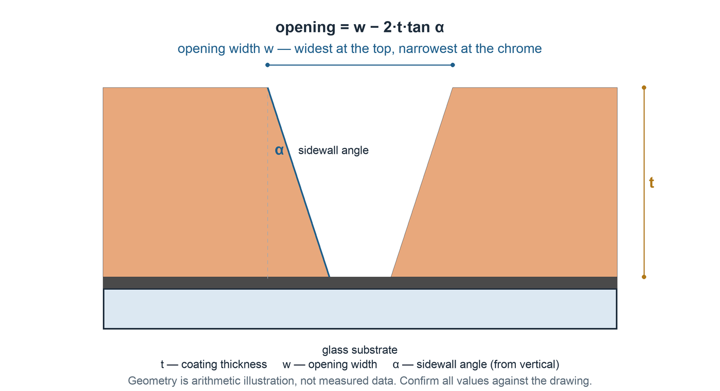
opening = w − 2·t·tan α. The factor of two is there because both walls contribute. What matters is that the loss is proportional to t: doubling the coating doubles the width error produced by a given wall angle.
| Coating t | 2° wall | 5° wall | 10° wall |
|---|---|---|---|
| 1 µm | 0.070 | 0.175 | 0.353 |
| 2 µm | 0.140 | 0.350 | 0.705 |
| 3 µm | 0.210 | 0.525 | 1.058 |
| 5 µm | 0.349 | 0.875 | 1.763 |
| 10 µm | 0.698 | 1.750 | 3.527 |
Read the 3 µm row against the published line-width tolerance. At 3 µm of coating and a 5° wall, the slope alone accounts for 0.52 µm of width change — larger than the whole ±0.2 µm window that the finished chrome line has to fit into. A wall angle of 5° is not a defect; it is an ordinary result of a process that has not been tuned for the feature. The point is that it becomes visible only when the coating is thick relative to the feature.
The ratio, not the thickness, sets the difficulty
Divide the coating by the smallest feature and the practical picture appears. Coatings near or below the feature size behave well: the developer reaches the bottom of the pattern quickly, the walls stay steep, and the dose has a wide margin. As the ratio grows, each of those becomes a tuning problem.
- Below 1:1 the resist is thinner than the feature. Resolution is limited by the exposure tool and the resist chemistry rather than by the coating.
- 1:1 to 3:1 is the usual working range for contact, proximity and direct-write processes on chrome blanks. A well-run thin-resist process sits here and holds sub-micrometre features.
- 3:1 to 6:1 is reachable, but the dose, bake and development have to be chosen for it. Expect to iterate on dose and development time rather than to inherit a recipe.
- Above 6:1 is thick-resist territory. Resist manufacturers report aspect ratios of roughly 6:1 to 10:1 for modern thick grades under optimised conditions — optimised being the operative word, and not something to assume on a first order.
Where your thickness sits in the published range
A 0.4–20 µm coating range is not one process with a dial. It spans families of resist with different viscosities, different photoactive content and different developer behaviour, and the useful part of each family is a narrower band than the range suggests.
Two practical consequences follow. First, "0.4 µm" and "20 µm" are not interchangeable options on the same job — they are different materials with different process windows, and a request that moves between them is a different process, not a different set point. Second, the thickness you ask for should be a value the chosen grade reaches comfortably, because a viscosity pushed to the edge of its range is where coating uniformity and edge bead problems appear.
A useful side note on spin coating: film thickness falls approximately with the square root of spin speed, so a fourfold change in speed gives roughly half the thickness. That leaves less range than most people expect from one resist, which is why resist grades exist at all. Industry reference, not a TL OPTIK specification.

What the coating changes after it is applied
Thickness is not a single decision with a single consequence. It propagates through the rest of the process, and each step has to absorb part of it:
- soft bake;
- exposure dose;
- development time;
- sidewall angle;
- width at the base of the resist;
- the chrome edge after etch.
The two that surprise people most are dose and development. A thicker film absorbs more of the exposure light before it reaches the bottom, so the dose that cleared a thin coating leaves resist behind in a thick one; and the developer has to work through the full depth, which lengthens the step and costs contrast at the same time. Resist manufacturers say the same thing from the other direction: their very thick grades exist precisely because pushing a thin resist to a thick film demands high doses, produces a poor wall profile and can generate nitrogen bubbles during exposure.
For chrome work there is a further consequence worth naming. Because the resist wall is transferred into the chromium during etch, the wall angle you develop is the profile the pattern edge inherits. A coating that is generous for the feature buys margin in coverage and handling; it costs profile.
A five-step way to choose
- Fix w first.Take the smallest line or space in the artwork, whichever is smaller. If the drawing contains both a 2 µm line and a 2 µm gap, w is 2 µm and the ratio applies to both.
- Set a ceiling on t/w.Work at or below 3:1 unless there is a reason to go higher and time to tune for it. A 1:1 target is a good default for a first order.
- Translate the ceiling into t.For w = 2 µm and a 1:1 target, that is about 2 µm of coating; for 1:1 at w = 1 µm, about 1 µm. Then check that the value is comfortably inside the chosen grade's range.
- Check the process, not just the number.Confirm the resist is sensitive at your exposure wavelength, that the developer is compatible, and that the bake step fits your handling time. A coating that is right on paper and wrong for the tool is still wrong.
- Write down how it will be measured.A target without a measurement method is not a requirement. How to fix that basis is covered under "How the coating is checked" below.
Where a drawing mixes feature sizes, the smallest one sets the coating. A 10 µm window will develop perfectly well in a resist chosen for a 1 µm line; the opposite is not true.
One product family, three supply stages
TL OPTIK supplies the same product family at three points in the chain — bare glass, chromium-coated glass, and resist-coated plate — and the coating question means something different at each.
- You buy a resist-coated plateThe thickness becomes your process input. State the target, the tolerance, the resist grade and tone, and the coating area, and confirm the soft-bake state you want to receive.
- You buy a finished patterned maskThe thickness becomes an internal choice inside the writing and etch route. What you specify is the smallest feature, the polarity and the width tolerance; the coating is selected to deliver them.
- You buy a chrome-coated blank, no resistThe coating question moves to your own line entirely. The relevant TL OPTIK parameters are the film family and the substrate, not the resist.
The published process order is the same in every case: substrate preparation, chromium sputtering, resist spin coating, soft bake, pattern exposure, development, chromium etch, resist strip and cleaning, then final inspection. Which of those steps sit on our side of the shipment is the only thing that changes.
What to put on the drawing
Coating requests that take an extra round of questions almost always omit the same two or three fields. The table below separates what a quotation needs from what production needs.
| Field | What to state | What it changes |
|---|---|---|
| Coating thickness | Target value and the tolerance you can accept; whether it is nominal or measured per plate | Aspect ratio, wall angle, dose and development time |
| Resist grade and tone | Model from the published list; positive or negative; dyed or undyed if it matters to you | Absorption at your wavelength, developer compatibility, achievable thickness band |
| Coating area | Coated region and any edge exclusion, especially where a fixture or mask frame will contact the plate | Usable area, edge bead handling, contact exposure clearance |
| Smallest line and space | The smaller of the two, in the artwork, for both polarities | Whether the requested coating is workable at all |
| Exposure route | Direct write, contact or proximity; wavelength in nanometres, not "UV" | Resist sensitivity match and the dose the coating will need |
| Bake state | Soft-baked on delivery, or coated only; agreed bake conditions if they are part of the specification | Adhesion, residual solvent, how long the plate can wait before exposure |
| Inspection basis | Measurement points, method and the record you expect with the plate | Whether the delivered thickness can be accepted without argument |
How the coating is checked
Thickness is a bulk property measured at points, not a picture of the whole plate. Three things therefore have to be agreed before the first part is inspected: where the measurement points are, how they are measured, and what record accompanies the plate.
Two points are rarely enough on a large plate. Coating thickness varies between the centre and the edge, and the edge is exactly where a contact frame or a mask holder will sit. A practical basis names a grid or a set of defined locations, a stated measurement method, and the reference conditions under which the values were taken — the same discipline that applies to any other dimensional requirement on the drawing.
For the acceptance side in more detail, see Inspection and acceptance of patterned glass, which covers how to define zones, defect significance and the conditions under which two measurements can be compared.
Common questions
Does a thicker photoresist make a better etch mask for chromium?
Rarely for chromium. The film being etched on a chrome-on-glass part is thin, so the resist is not acting as a deep-etch mask. Thickness is chosen for the profile it produces and for coverage and handling margin, not for etch depth.
Can one coating thickness serve every feature on my drawing?
Usually yes, because the smallest feature sets the coating and larger features are unaffected by a thinner resist. The reverse does not hold: a coating chosen for 10 µm windows will not hold a 1 µm line with a usable wall angle.
What thickness tolerance should I ask for?
State a target value, the tolerance you can accept and how the coating will be measured. The published range of 0.4–20 µm describes what can be coated; the tolerance and uniformity for a specific grade are confirmed in writing against the drawing rather than assumed from that range.
Will the resist thickness change the measured line width?
Indirectly, through the wall angle. A sloped wall moves the pattern edge between the top of the resist and the chrome below it. The finished chrome line width is a separate requirement and is agreed on the drawing.
Can you coat a 9-inch or non-square plate?
The published coating formats are 3, 4, 5, 6 and 7 inch squares on soda-lime or white crown glass. Larger and non-square formats are a development question: send the outline, thickness and coating area so the route can be reviewed before it is quoted.
How is the coating checked before shipment?
Thickness is measured as part of the inspection plan agreed for the order, which should name the measurement points, the method and the record format. No default sampling plan is published, because the acceptance basis is set by the drawing and the quality agreement.
Send the smallest feature, not just the thickness
A coating can be quoted faster when the smallest line or space arrives with it. Include the outline, substrate, thickness target, resist grade or tone, coating area and the exposure wavelength.