
Photosensitive starting blanks for laser-written mask fabrication.
Photoresist-Coated Chrome Plates
Photoresist-coated photomask blanks made by DC magnetron sputtering and spin coating, for display, semiconductor, optical and circuit-patterning applications.
Prepared for your next exposure.
Photoresist coatedCustom formats
Product selection
What it is and what it does
Our multilayer coating option uses DC magnetron sputtering to deposit chromium oxynitride / chromium nitride / chromium oxynitride, followed by photoresist spin coating. Subsequent exposure, development, chromium-film etching and resist removal produce the finished mask pattern.
When to choose it
Choose the supply stage that matches the processes you perform in-house: bare glass before coating, chromium-coated glass before resist coating, or a resist-coated plate before exposure.
How it differs from related products
A resist-coated blank is ready for a compatible exposure step, not a finished photomask. Resist tone, spectral sensitivity and development chemistry affect its suitability for the writer; chromium provides the final opaque pattern after etching.
What can be customised
Glass or fused silica, chromium stack, resist family and thickness, edge exclusion and usable exposure field form the configuration.
What you receive
The supplied item is an unpatterned substrate or coated blank in the selected process state. A finished reticle, encoder track or exposure mask requires a subsequent patterning step. Handling, storage and any accompanying inspection data depend on the selected coating and order.
Specifications and inspection
Product configuration
| Substrate | Double-side-polished soda-lime or white crown glass |
|---|---|
| Square formats | 3 / 4 / 5 / 6 / 7 in |
| Chrome film families | LRC / HRC / BCB |
| Photoresist options | AZ 1500 / IP 3500 / AZ TFP650; additional positive-resist grades listed below |
| Resist thickness | 0.4–20 µm depending on resist model; fixed-thickness grades also available |
Small-format blank dimensions
Both substrate surfaces are polished. S = soda-lime glass; WC = white crown glass. Dimensional limits and flatness apply to the individual format and material listed below.
| Format code | Material | Nominal format (in) | Side length (mm) | Thickness (mm) | Flatness (µm) |
|---|---|---|---|---|---|
| 3004 | S | 3 × 3 | 75.4–76.2 | 0.90–1.05 | ≤5 |
| 3006 | S | 3 × 3 | 75.4–76.2 | 1.40–1.60 | ≤5 |
| 3006 | WC | 3 × 3 | 75.4–76.2 | 1.50–1.55 | ≤20 |
| Format code | Material | Nominal format (in) | Side length (mm) | Thickness (mm) | Flatness (µm) |
|---|---|---|---|---|---|
| 4004 | S | 4 × 4 | 100.8–101.6 | 0.90–1.05 | ≤5 |
| 4004 | WC | 4 × 4 | 100.95–101.45 | 0.97–1.03 | ≤20 |
| 4006 | S | 4 × 4 | 100.8–101.6 | 1.40–1.55 | ≤5 |
| 4006 | WC | 4 × 4 | 100.8–101.6 | 1.45–1.55 | ≤20 |
| 4008 | S | 4 × 4 | 100.8–101.6 | 1.95–2.05 | ≤5 |
| 4008 | WC | 4 × 4 | 100.8–101.6 | 2.00–2.05 | ≤20 |
| 4009 | S | 4 × 4 | 100.8–101.6 | 2.20–2.40 | ≤5 |
| 4009 | WC | 4 × 4 | 100.8–101.6 | 2.30–2.40 | ≤5 |
| 4010 | S | 4 × 4 | 100.8–101.6 | 2.44–2.64 | ≤5 |
| 4010 | WC | 4 × 4 | 100.8–101.6 | 2.50–2.60 | ≤20 |
| 4012 | S | 4 × 4 | 100.8–101.6 | 2.95–3.05 | ≤5 |
| 4012 | WC | 4 × 4 | 100.8–101.6 | 2.95–3.00 | ≤20 |
| 4016 | WC | 4 × 4 | 100.8–101.6 | 4.00–4.05 | ≤20 |
| 4018 | WC | 4 × 4 | 100.8–101.6 | 4.50–4.55 | ≤20 |
| 4020 | WC | 4 × 4 | 101.2–101.4 | 4.90–5.00 | ≤20 |
| Format code | Material | Nominal format (in) | Side length (mm) | Thickness (mm) | Flatness (µm) |
|---|---|---|---|---|---|
| 5002 | S | 5 × 5 | 126.2–127.0 | 0.45–0.55 | ≤20 |
| 5002 | WC | 5 × 5 | 126.2–127.0 | 0.45–0.55 | ≤20 |
| 5004 | S | 5 × 5 | 126.2–127.0 | 0.95–1.05 | ≤20 |
| 5004 | WC | 5 × 5 | 126.2–127.0 | 0.95–1.05 | ≤20 |
| 5006 | WC | 5 × 5 | 126.2–127.0 | 1.45–1.55 | ≤20 |
| 5008 | WC | 5 × 5 | 126.2–127.0 | 2.00–2.05 | ≤20 |
| 5009 | S | 5 × 5 | 126.2–127.0 | 2.20–2.40 | ≤8 |
| 5012 | WC | 5 × 5 | 126.2–127.0 | 2.95–3.05 | ≤20 |
| 5014 | WC | 5 × 5 | 126.2–127.0 | 3.45–3.55 | ≤20 |
| Format code | Material | Nominal format (in) | Side length (mm) | Thickness (mm) | Flatness (µm) |
|---|---|---|---|---|---|
| 6009 | S | 6 × 6 | 151.6–152.4 | 2.20–2.40 | ≤10 |
| 6009 | WC | 6 × 6 | 151.75–152.25 | 2.30–2.40 | ≤20 |
| 6012 | S | 6 × 6 | 151.6–152.4 | 2.95–3.15 | ≤10 |
| 6023 | S | 6 × 6 | 151.6–152.4 | 5.75–5.95 | ≤10 |
| 6025 | S | 6 × 6 | 151.6–152.4 | 6.25–6.45 | ≤10 |
| Format code | Material | Nominal format (in) | Side length (mm) | Thickness (mm) | Flatness (µm) |
|---|---|---|---|---|---|
| 7009 | S | 7 × 7 | 177.0–177.8 | 2.20–2.40 | ≤15 |
| 7012 | S | 7 × 7 | 177.0–177.8 | 2.95–3.15 | ≤15 |
| 7012 | WC | 7 × 7 | 177.0–177.8 | 2.95–3.15 | ≤30 |
Chromium film specifications
Select the film type by optical density, reflectance and pattern-transfer requirements. LRC = low-reflective chrome; HRC = high-reflective chrome; BCB = blue-chrome-blue. Film thickness is expressed in nm (1 nm = 10 Å).
| Film type | Coating family | Film thickness (nm) | Optical density / wavelength | Reflectance / wavelength | Wet etch time (s) |
|---|---|---|---|---|---|
| Type-1 | LRC | 100 ± 8 | 3.1 ± 0.2 @ 450 nm | 11 ± 2% @ 436 nm | 43–53 |
| Type-2 | LRC | 125 ± 10 | 4.0 ± 0.2 @ 450 nm | 11 ± 2% @ 436 nm | 50–60 |
| Type-3 | BCB | 200 ± 20 | 5.0 ± 0.3 @ 450 nm | ≤7% @ 600 ± 50 nm | >70 |
| Type-4 | LRC | 200 ± 20 | 5.0 ± 0.3 @ 450 nm | 11 ± 2% @ 436 nm | >70 |
| Type-5 | HRC | 100 ± 10 | 3.1 ± 0.2 @ 550 nm | ≥45% @ 436 nm | 43–53 |
| Type-6 | BCB | 250 ± 20 | 5.0 ± 0.3 @ 500 nm | ≤7% @ 600 ± 50 nm | >70 |
| Type-7 | LRC | 125 ± 10 | 3.1 ± 0.2 @ 550 nm | 11 ± 2% @ 436 nm | 50–60 |
| Type-8 | HRC | 200 ± 20 | 5.0 ± 0.3 @ 550 nm | ≥45% @ 436 nm | >70 |
Wet etch times are measured by immersion with stirring at 20 ± 0.1 °C, using 200 g ceric ammonium nitrate and 35 mL glacial acetic acid, with deionized water to a total volume of 1000 mL. The bilateral undercut rate is <0.07 µm per 10 s, excluding BCB.
| Coating family | 98% H₂SO₄ at 120 °C | 98% H₂SO₄ + H₂O₂ at 75 °C |
|---|---|---|
| LRC / HRC | >120 min | >120 min |
| BCB | >60 min | >60 min |
Optical properties are measured on one witness sample per lot. Film thickness is measured by step profilometry; optical density by densitometry; reflectance by spectrophotometry.
Photoresist-coated chrome plates, also called resist-coated photomask blanks, are photosensitive starting materials for photomask fabrication. They combine a cleaned glass substrate, a sputtered chromium-based film stack and a spin-coated photoresist layer.
Built for your process.
Request a Quote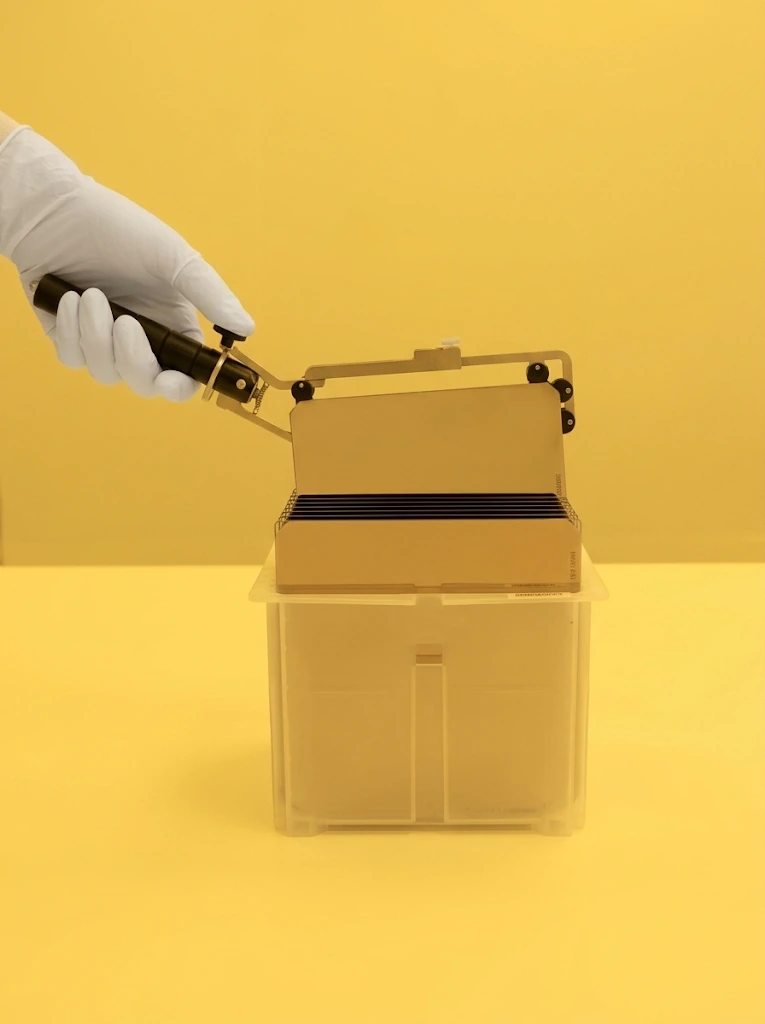
How a resist-coated photomask blank is made
The manufacturing sequence starts with a thoroughly cleaned substrate. DC magnetron sputtering forms the selected chromium-based coating, and spin coating applies the photosensitive resist. The resist is the light-sensitive layer; the chromium-based film becomes the optical pattern after etching.
| Layer / material | Function and selection |
|---|---|
| Glass substrate | Cleaned substrate selected for format, flatness and optical transmission. |
| Chromium oxynitride / chromium nitride / chromium oxynitride | Sputtered film stack configured for optical density, reflectance and pattern-transfer requirements. |
| Photoresist | Spin-coated photosensitive layer selected for the exposure method, film thickness and development process. |
This oxynitride/nitride stack is one available coating configuration. Specify the selected stack, optical density and reflectance separately from photoresist chemistry and thickness. The stack description does not prescribe individual layer thicknesses or apply automatically to every LRC, HRC or blue-chromium option.
Applications of the finished mask and patterned component
Select the blank around the photomask or component that will be made from it. The same material category supports different industries, while the required format, feature size, registration and defect grade depend on the specific exposure process.
| Industry | Typical applications | Role of the blank |
|---|---|---|
| Flat-panel displays | TFT-LCD, OLED, color filters (CF) and touch panels (TP); STN/CSTN LCD and plasma display panel (PDP) processes where required. | Masks for repeated electrode, pixel and other functional patterns, with format and registration matched to the exposure process. |
| Semiconductors & MEMS | Integrated circuits (including LSI/VLSI), transistors and discrete devices, LEDs, MEMS and IC bumping. | Photomasks for device and packaging patterning. Specify the lithography tool, mask scale, minimum features and defect criteria for the particular process. |
| Precision optics & metrology | Optical encoder discs, calibration targets, optical gratings and other patterned optical components. | Masks for pattern transfer, or a coated starting substrate for direct patterning of the optical component itself. |
| Circuit boards & interconnects | High-density interconnect PCBs (HDI), flexible printed circuits (FPC) and lead frames. | Rigid glass phototools for compatible imaging and etching processes. Define artwork polarity, dimensional stability and registration needs. |
Cleanroom manufacturing & contamination control
Our manufacturing and inspection facilities include cleanroom areas ranging from Class 10 to Class 100,000, expressed in the traditional cleanroom classification terminology. Controlled environments help reduce particle contamination during substrate preparation, coating, handling and inspection.
Cleanroom classification describes the environment. Finished-blank acceptance also depends on substrate defects, chromium pinholes, optical properties and resist thickness uniformity. Specify these product requirements alongside any cleanroom-class requirement for your project.
Quality & InspectionWhere it fits in the process
Choose a photoresist-coated chrome plate when the substrate should arrive prepared for laser direct writing or another agreed exposure route.
Photoresist specifications
| Grade | Photoresist | Resist thickness (nm) | Thickness uniformity | Coated area |
|---|---|---|---|---|
| High Grade | AZ 1500 | 500 | ±1% | Square or circular |
| Standard Grade | AZ 1500 | 500 | ±2% | Square or circular |
| High Grade | IP 3500 | 460 | ±1% | Circular |
| Standard Grade | AZ TFP650 | 700 | ±3% | Square or circular |
| Standard Grade | AZ TFP650 | 1000 | ±3% | Square or circular |
Resist thickness and uniformity are measured on one witness sample per lot. Every plate receives visual resist inspection under yellow illumination, using a 120,000 lux halogen lamp 15 cm from the substrate.
Recommended development: AZ 300 MIF (2.38%), 23 °C, 60 s. Exposure settings and process adjustments follow the selected resist and pattern.
Substrate finish and defect limits
| Property | Specification |
|---|---|
| Squareness | 90° ± 5′ |
| Edge chamfer | 45° |
| Bevel width, thickness ≤1.6 mm | 0.20–0.50 mm |
| Bevel width, thickness >1.6 mm | 0.40–0.80 mm |
| Corner radius | 2.00–3.00 mm |
| Effective inspection area | Square side D = L − 12.7 mm, where L is the plate side length. |
| Defect | Acceptance limit |
|---|---|
| Cracks / chips | No defects >2 mm in the effective area |
| Bubbles / inclusions | No defects >5 µm |
| Pits | No defects >5 µm |
| Scratches | Limit: 5 µm × 1 mm in the effective area |
Glass appearance inspection uses a 120,000 lux halogen inspection lamp at a distance of 15 cm from the substrate.
| Grade | Pinhole size | Acceptance limit |
|---|---|---|
| High Grade | <2 µm | No limit |
| High Grade | 2–5 µm | ≤0.3 / in² |
| High Grade | >5 µm | None permitted |
| Standard Grade | >2 µm | ≤0.5 / in² |
| Standard Grade | >5 µm | None permitted |
| BCB | >5 µm | ≤0.5 / in² |
| BCB | >10 µm | None permitted |
Every plate undergoes pinhole inspection. Defect density and the no-defect size limit both apply to the selected grade.
Packaging, traceability and storage
| Property | Specification |
|---|---|
| Packaging | Black protective box, aluminium foil and PE film, vacuum packaged to protect against light and contamination. |
| Lot traceability | Chrome sputtering operator, production date, coating equipment, box number and inspector. |
| Box label | Product model, quantity / product report and lot ID. |
| Photoresist quality assurance period | 3 months for photoresist critical-dimension (CD) characteristics and defect quality under the specified storage conditions. |
| Storage temperature | 20 ± 5 °C |
| Relative humidity | 45 ± 5% RH |
Positive photoresist options: thin and thick films
Choose the photoresist family and target film thickness for the exposure and pattern-transfer process. The extended ranges below complement the fixed-thickness, high-uniformity grades already listed; they are not one universal coating specification.
| Photoresist model | Available thickness (µm) | Uniformity at thickness ≤1 µm | Uniformity at thickness >1 µm |
|---|---|---|---|
| AZ 4562 | 2–20 | Not applicable | 10% |
| AZ 4620 | 2–20 | Not applicable | 10% |
| AZ 1500 | 0.5–3 | 1% | 5% |
| AZ TFP650F5 | 0.5–10 | 1% | 5% |
| GRX M237 | 0.5–1 | 1% | Not applicable |
| THMR IP3500 | 0.4–1 | 1% | Not applicable |
Select the uniformity column only within the listed thickness range. For example, AZ 4562 and AZ 4620 start at 2 µm and therefore use the >1 µm column. GRX M237 and THMR IP3500 stop at 1 µm, so no thicker-film uniformity is assigned.
The extended table states uniformity percentages without a ± convention or calculation formula. Define the uniformity calculation, sampling positions and edge exclusion in the inspection specification. Keep the full model suffix when ordering; AZ TFP650F5 is not silently substituted for the previously listed AZ TFP650 configuration.
Developer selection for coated blanks
Developer chemistry is part of the coated-blank process specification. The options below describe process compatibility, not a separate chemical product supplied with every blank. Choose the developer using the exact resist grade and its current technical data sheet.
| Developer | Chemistry / role |
|---|---|
| Aqueous NaOH / KOH developer | Inorganic alkaline system; formulation specified for the resist |
| AZ 400K | Inorganic alkaline developer option for thick positive resist; dilution follows the resist process |
| AZ 300 MIF | Metal-ion-free, aqueous 2.38% TMAH; surfactant-free option |
| AZ 600 MIF | Metal-ion-free, aqueous 2.38% TMAH; surfactant-containing option |
Development time and temperature depend on film thickness, exposure and agitation. The existing 23 °C / 60 s AZ 300 MIF recommendation belongs to its specified thin-film process; it is not a universal recipe for the 2–20 µm thick-resist range.
Chromium-film pinhole grades by substrate format
A pinhole in this specification is an unintended transparent defect in the chromium film. It is not a designed optical aperture and does not indicate a hole through the glass. Select the format and coating acceptance grade together.
| Acceptance grade | Rejected pinhole sizes |
|---|---|
| Standard Grade | d ≥5 µm |
| Premium Grade | d ≥1 µm |
These thresholds define the rejected defect sizes. The inspection specification must also define any permitted defect count below the threshold and the inspected area.
| Acceptance grade | Defect size, d | Acceptance limit |
|---|---|---|
| A | 5 ≤ d < 10 µm | ≤0.01 / cm² |
| A | d ≥ 10 µm | None permitted |
| B | 5 ≤ d < 10 µm | ≤0.01 / cm² |
| B | 10 ≤ d < 30 µm | ≤0.003 / cm² |
| B | d ≥ 30 µm | None permitted |
| C | 5 ≤ d < 10 µm | ≤0.01 / cm² |
| C | 10 ≤ d < 50 µm | ≤0.003 / cm² |
| C | d ≥ 50 µm | None permitted |
The no-defect threshold takes precedence at the boundary of each size band. For example, Grade B rejects all pinholes of 30 µm or larger. Specify inspected area, edge exclusions and the count-rounding rule for area-based density limits. No acceptance value is assigned here to pinholes smaller than 5 µm.
What can be customized
- Photoresist chemistry and polarity
- Target resist thickness and coating area
- Exposure wavelength and development route
- Soft-bake, cleanliness and handling requirements
Where this product is used
Resist-coated blanks for the display-mask fabrication step.
Starting material for making the glass phototool.
Resist-coated starting blanks for teams making their own masks.
Common questions
Is a resist-coated blank already a finished photomask?
No. The blank carries the photosensitive coating but has not yet been patterned. Exposure and subsequent pattern-transfer steps turn it into a photomask. The listed industries describe the uses of those finished masks and patterned components.
Which photoresists are available?
Fixed-thickness grades include AZ 1500, IP 3500 and AZ TFP650. Additional options include AZ 4562, AZ 4620, AZ TFP650F5, GRX M237 and THMR IP3500. Select the exact model, thickness and uniformity specification from the tables below.
What information is needed for quotation?
Include substrate, dimensions, resist type or polarity, target thickness, exposure method and quantity.
Selection notes
Photoresist-coated chrome plates combine a glass substrate, chromium-based film and pre-applied resist for a compatible exposure process.
Choose resist model, tone, thickness, sensitivity range and developer chemistry together with the exposure equipment. Plate size alone does not define process compatibility.
Information for your inquiry
Substrate format, resist model and thickness, exposure method, coated area, edge-bead exclusion and quantity.
How does a coated plate differ from a finished mask?
The coated plate is a prepared process material. A finished mask already contains the drawing-defined transparent and opaque regions. Choose according to whether you will fabricate or use the pattern.