What the component does
The patterned mask controls where exposure light reaches the resist. An unpatterned chrome blank is an input to mask fabrication, not a finished exposure tool.
Transfer a controlled pattern into photoresist and relate each exposure to the wafer alignment references.
This illustrates proximity exposure. Contact exposure closes the gap; projection exposure adds imaging optics.
Layer registration and feature inspection are separate checks after pattern transfer.
The patterned mask controls where exposure light reaches the resist. An unpatterned chrome blank is an input to mask fabrication, not a finished exposure tool.
Mask orientation, resist polarity and alignment marks must agree with the exposure process. Subsequent development and etching determine the transferred structure.
Excessive gap, particles or artwork registration errors can change feature edges or layer placement. Mask feature size is not automatically the final device dimension.
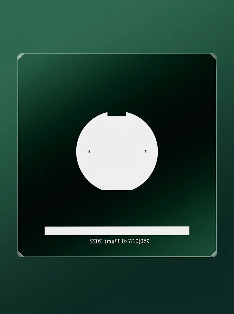
Finished masks on a low-expansion substrate.
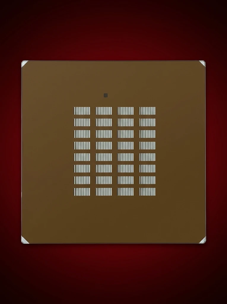
Coordinated layers with shared alignment datums.
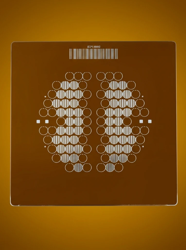
Masks for exposure with the patterned surface at the workpiece.
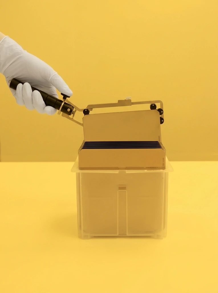
Photosensitive starting blanks for laser-written mask fabrication.
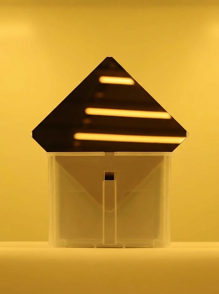
Unpatterned fused-silica blanks for subsequent resist coating and mask making.
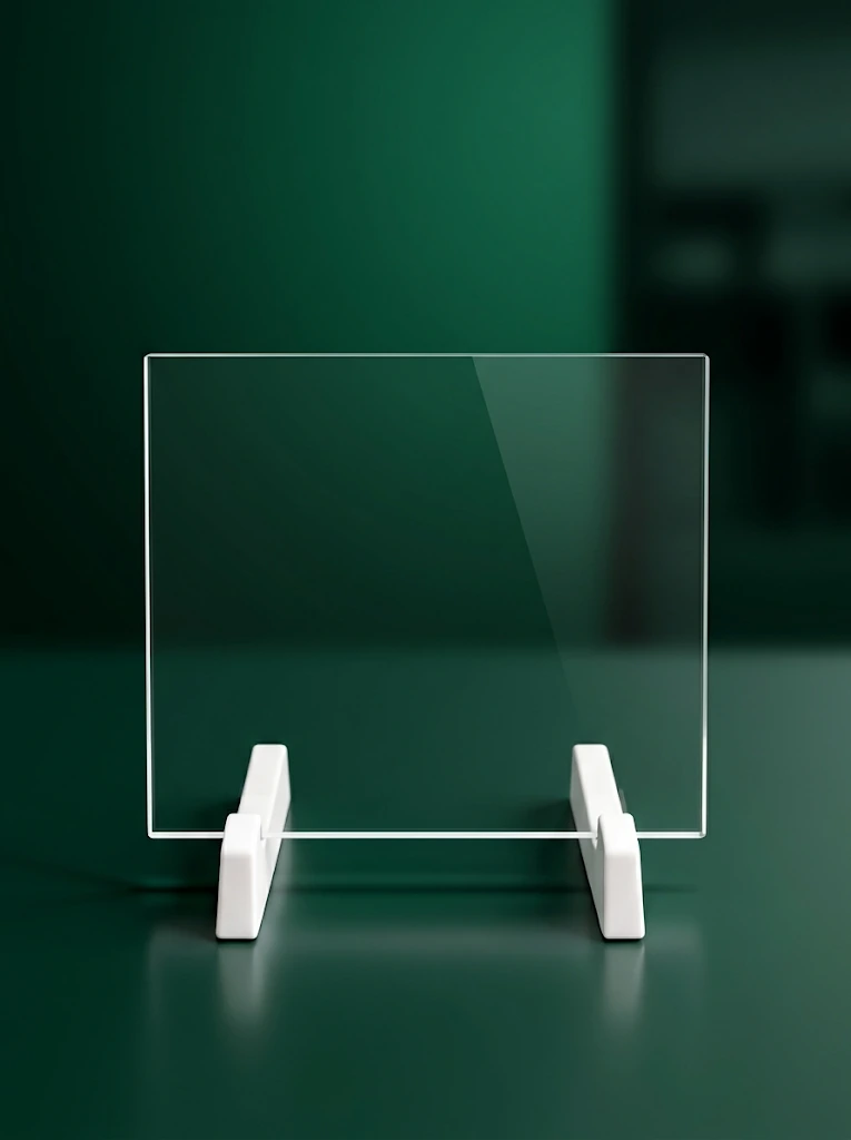
Uncoated substrates where UV transmission and thermal stability matter.

Masks for a specified exposure gap.

Registration markers for equipment and optical inspection setups.
Photolithography transfers a mask pattern into resist on a workpiece. A resist-coated blank is the starting material for making that mask, while a finished photomask carries the image used during exposure. Separate calibration or fiducial components can support inspection and alignment of the equipment.
Match substrate transmission, mask scale and feature requirements to the lithography tool. Contact and proximity exposure differ in gap and pattern-transfer behaviour. A multi-layer device also needs consistent datums and alignment marks across masks. Material choice alone does not establish suitability for a particular process node.
A photomask defines where a resist is exposed. Development and subsequent etching or deposition transfer the intended geometry into a process layer. Electrode layouts, contact openings and wafer-level interconnect patterns each need artwork, polarity and alignment references matched to that layer.
In mask-based semiconductor processing, photomasks define exposure regions and alignment marks relate successive patterns to shared coordinates.
Prepared resist-coated plates serve mask fabrication; finished masks serve pattern transfer. Select these supply states separately.
Transfer also depends on exposure gap, resist, development and later processing. Define the required mask geometry and process bias in the artwork.