
Unpatterned fused-silica blanks for subsequent resist coating and mask making.
Chrome-on-Fused-Silica Photomask Blanks
Chrome-on-fused-silica blanks for UV lithography, microfabrication and high-stability photomask applications.
Precision chrome on fused silica.
Chrome-coated blanksCustom formats
Product selection
What it is and what it does
This configuration is selected when substrate stability and the optical behavior of the fused silica matter together with the chrome patterning process. Film, surface and dimensional requirements should be confirmed against the exposure system and the final pattern.
When to choose it
Choose the supply stage that matches the processes you perform in-house: bare glass before coating, chromium-coated glass before resist coating, or a resist-coated plate before exposure.
How it differs from related products
It combines an unpatterned chrome film with a fused-silica substrate. Compared with a finished fused-silica mask, patterning remains to be done; compared with a glass blank, the material changes thermal and spectral behaviour.
What can be customised
Material grade, outline, thickness, polished area and edge finish define the substrate. Coated versions also allow a film stack and resist preparation matched to the downstream exposure and etching process.
What you receive
The supplied item is an unpatterned substrate or coated blank in the selected process state. A finished reticle, encoder track or exposure mask requires a subsequent patterning step. Handling, storage and any accompanying inspection data depend on the selected coating and order.
Specifications and inspection
Product configuration
| Product type | Unpatterned chrome-on-fused-silica blank |
|---|---|
| Substrate | Fused silica, grade and spectral range to specification |
| Chrome layer | Deposited chromium; thickness and optical target to specification |
| Geometry | Size, thickness, flatness, parallelism and edge condition |
| Next process | Photoresist coating, laser writing or mask exposure |
Fused silica substrate specifications
| Property | Specification |
|---|---|
| Material | Synthetic fused silica |
| Square formats | 3 / 4 / 6 / 7 / 8 / 9 in |
| Thickness | ≥0.3 mm |
| Total thickness variation (TTV) | ≤2 µm |
| Flatness | ≤2 µm |
Chromium film specifications
Select the film type by optical density, reflectance and pattern-transfer requirements. LRC = low-reflective chrome; HRC = high-reflective chrome; BCB = blue-chrome-blue. Film thickness is expressed in nm (1 nm = 10 Å).
| Film type | Coating family | Film thickness (nm) | Optical density / wavelength | Reflectance / wavelength | Wet etch time (s) |
|---|---|---|---|---|---|
| Type-1 | LRC | 100 ± 8 | 3.1 ± 0.2 @ 450 nm | 11 ± 2% @ 436 nm | 43–53 |
| Type-2 | LRC | 125 ± 10 | 4.0 ± 0.2 @ 450 nm | 11 ± 2% @ 436 nm | 50–60 |
| Type-3 | BCB | 200 ± 20 | 5.0 ± 0.3 @ 450 nm | ≤7% @ 600 ± 50 nm | >70 |
| Type-4 | LRC | 200 ± 20 | 5.0 ± 0.3 @ 450 nm | 11 ± 2% @ 436 nm | >70 |
| Type-5 | HRC | 100 ± 10 | 3.1 ± 0.2 @ 550 nm | ≥45% @ 436 nm | 43–53 |
| Type-6 | BCB | 250 ± 20 | 5.0 ± 0.3 @ 500 nm | ≤7% @ 600 ± 50 nm | >70 |
| Type-7 | LRC | 125 ± 10 | 3.1 ± 0.2 @ 550 nm | 11 ± 2% @ 436 nm | 50–60 |
| Type-8 | HRC | 200 ± 20 | 5.0 ± 0.3 @ 550 nm | ≥45% @ 436 nm | >70 |
Wet etch times are measured by immersion with stirring at 20 ± 0.1 °C, using 200 g ceric ammonium nitrate and 35 mL glacial acetic acid, with deionized water to a total volume of 1000 mL. The bilateral undercut rate is <0.07 µm per 10 s, excluding BCB.
| Coating family | 98% H₂SO₄ at 120 °C | 98% H₂SO₄ + H₂O₂ at 75 °C |
|---|---|---|
| LRC / HRC | >120 min | >120 min |
| BCB | >60 min | >60 min |
Optical properties are measured on one witness sample per lot. Film thickness is measured by step profilometry; optical density by densitometry; reflectance by spectrophotometry.
Chrome-on-fused-silica photomask blanks combine a low-expansion fused silica substrate with a precision chromium film for demanding pattern-transfer applications.
Built for your process.
Request a Quote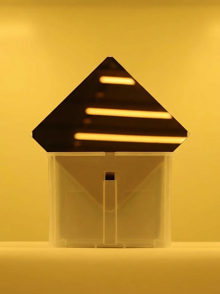
Where it fits in the process
Choose this configuration when fused silica behavior and a chromium patterning layer must be controlled together in one blank.
Small-format substrate flatness options
Choose the format code, glass material and flatness limit together. Each number below is a selectable maximum flatness in micrometres, not a thickness tolerance or a minimum-to-maximum range. These format-based options are separate from the precision-grade specifications above and the coated-blank dimensional schedules.
| Format code | Fused silica: available flatness limits (µm) |
|---|---|
| 4004 | 2 / 5 / 6 / 10 |
| 4006 | 2 / 5 / 6 / 10 |
| 4009 | 2 / 5 / 6 / 10 |
| 5006 | 2 / 5 / 6 / 10 |
| 5009 | 2 / 5 / 6 / 10 |
| 6009 | 2 / 5 / 6 / 10 |
| 6012 | 2 / 5 / 6 / 10 |
| 6025 | 2 / 5 / 6 / 10 |
| 7010 | 2 / 5 / 6 / 10 |
| 7012 | 2 / 5 / 6 / 10 |
| Property | Specification |
|---|---|
| Edge preparation | Ground edges with a 45° chamfer |
| Edge squareness: linear deviation / reference length | <0.015 in / 1 in |
| Face-to-face thickness difference | |A − B| <5 µm |
The linear squareness option is separate from the 90° ±5′ blank-edge specification. The A/B requirement compares thickness at two specified locations and does not replace a full-aperture TTV measurement. Identify the selected edge specification, measurement positions, clear aperture and flatness test method on the drawing.
Chromium-film pinhole grades by substrate format
A pinhole in this specification is an unintended transparent defect in the chromium film. It is not a designed optical aperture and does not indicate a hole through the glass. Select the format and coating acceptance grade together.
| Acceptance grade | Rejected pinhole sizes |
|---|---|
| Standard Grade | d ≥5 µm |
| Premium Grade | d ≥1 µm |
These thresholds define the rejected defect sizes. The inspection specification must also define any permitted defect count below the threshold and the inspected area.
What can be customized
- Fused silica material and optical range
- Chrome thickness, density and reflectivity
- Dimensions, flatness and surface quality
- Resist compatibility, cleaning and packaging
Where this product is used
Common questions
When should I choose a chrome-on-fused-silica blank?
Use it when fused silica stability or UV behavior is important to the patterning and exposure process.
Can it be supplied photoresist coated?
Yes, when the resist type, thickness and exposure route are defined.
Are the dimensions standard?
Dimensions and tolerances are confirmed from the project drawing or mask format.
Selection notes
Chrome-on-fused-silica blanks combine a fused silica substrate with a chromium film for later photolithographic patterning.
Choose film opacity, surface and defect requirements together with the working spectrum and substrate dimensional stability.
Information for your inquiry
Silica grade, outline, thickness, chromium stack, exposure wavelength, resist state and inspection requirements.
Is this a finished fused silica photomask?
It is an unpatterned coated material. A finished mask has already been processed to the approved artwork; specify the supply state that matches your manufacturing step.