What the component does
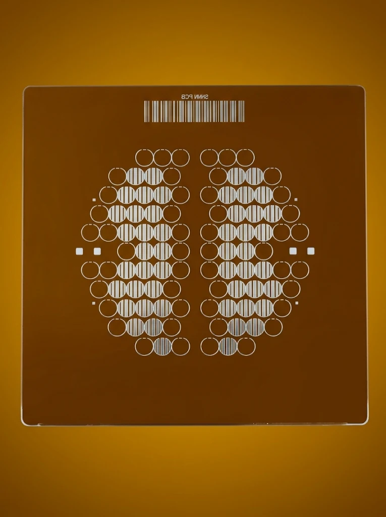
A coordinated mask set defines where successive layers are exposed. It can support compatible microfluidic, sensor and microstructure development routes.
Coordinate multiple lithography steps so that microstructures, openings and alignment features share a consistent geometry.
A mask defines a two-dimensional exposure pattern. Etch depth and sidewall shape come from the subsequent fabrication route.
This simplified section illustrates registration and depth as separate design variables, without implying a particular MEMS device.
A coordinated mask set defines where successive layers are exposed. It can support compatible microfluidic, sensor and microstructure development routes.
Keep layer names, mask side, polarity, alignment marks and revision control consistent. Front-to-back alignment needs a process designed for that task.
Overlay errors can obstruct openings or misplace interacting structures. Reducing the smallest line alone does not guarantee functional devices or successful release.
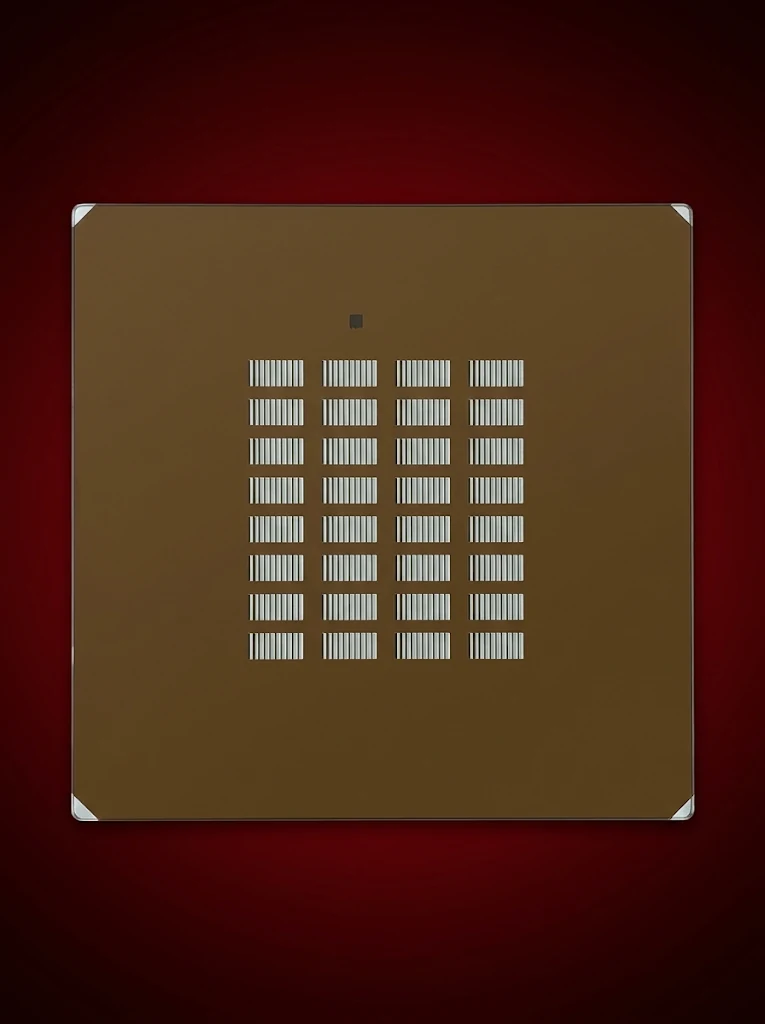
Coordinated mask layers for shared alignment and artwork revision control.
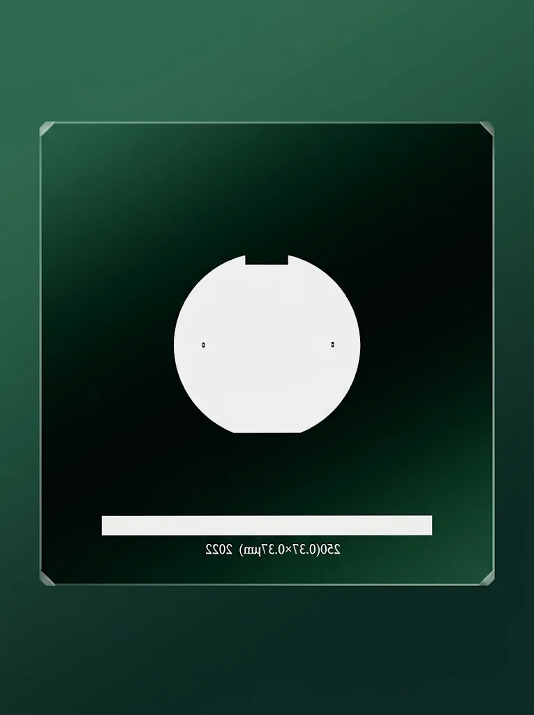
Patterned chromium masks on fused silica for a compatible exposure process.
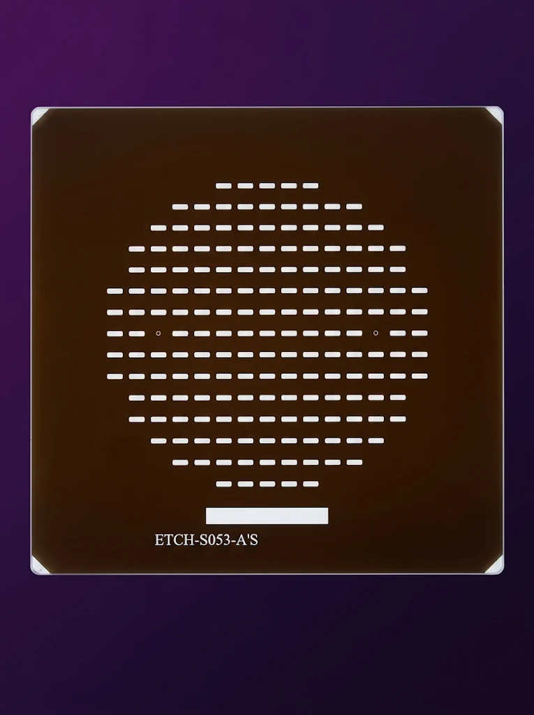
Pattern transfer with the exposure gap defined by the process.
Pattern transfer in contact-exposure workflows.
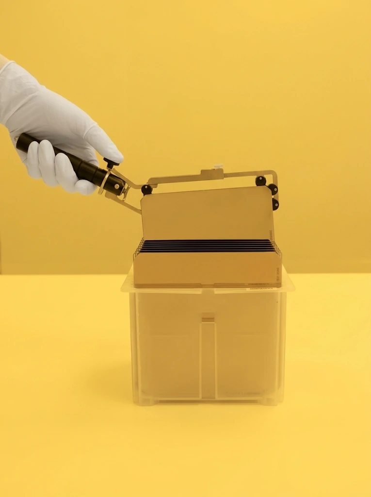
Resist-coated starting blanks for teams making their own masks.
MEMS means micro-electro-mechanical systems: small devices that combine mechanical structures with electrical sensing or actuation. Pressure sensors, inertial sensors and micromirrors are familiar examples. Photolithography can define electrodes, structural boundaries and process openings before subsequent material processing forms the device.
Start with the exposure tool and the purpose of each mask layer. Specify the substrate, pattern polarity, usable field and alignment marks around the selected process. TL OPTIK supplies mask blanks and patterned optical components for these steps; the device manufacturer defines the etching, deposition, release and assembly process.
Sensors may convert pressure, acceleration or movement into an electrical response; actuators use an input to create motion. Depending on the device architecture, masks define electrode regions, structural layers or access openings. A well-defined mask gives the process a repeatable geometry to transfer.
A mask set maintains a consistent coordinate origin, layer identification and alignment-mark scheme. This helps the process team relate successive exposures and identify each approved artwork revision. Finished-device overlay also depends on the exposure tool, substrate and process conditions.
Related lithography workflows use masks to define channel layouts, mould features or test structures. The mask carries the two-dimensional exposure geometry; resist processing and subsequent replication or etching determine the resulting depth and three-dimensional form.
Review clear and opaque regions, layer names, orientation and critical pattern areas before mask manufacture. Keeping the drawing revision and inspection requirements tied to each mask helps a development team repeat an experiment or transfer an approved design into later production.
MEMS mask sets relate successive exposures to shared coordinates. Each mask defines a two-dimensional exposure region.
Later material processing determines depth, sidewalls and release. Provide the mask layer data separately from the final 3D structure.
Also provide the 2D artwork for each exposure, layer order, film side and alignment convention. The 3D drawing explains the goal but does not replace layer data.