What the component does
The mask supplies a repeatable optical master for compatible resist patterning. The same principle can support circuit and lead-frame workflows with different artwork.
Transfer conductor, opening or lead-frame artwork into a resist process with a consistent orientation and registration reference.
Contact and proximity routes use different spacing conditions; the drawing shows an illustrative open gap.
Development and etching follow exposure. Their process bias must be considered separately from mask geometry.
The mask supplies a repeatable optical master for compatible resist patterning. The same principle can support circuit and lead-frame workflows with different artwork.
Pattern polarity, viewed side and front-to-back registration must agree with the manufacturing sequence, particularly for double-sided designs.
A mirrored file or incorrect polarity can produce an unusable pattern. Flexible-material movement can introduce registration error even with an accurate mask.
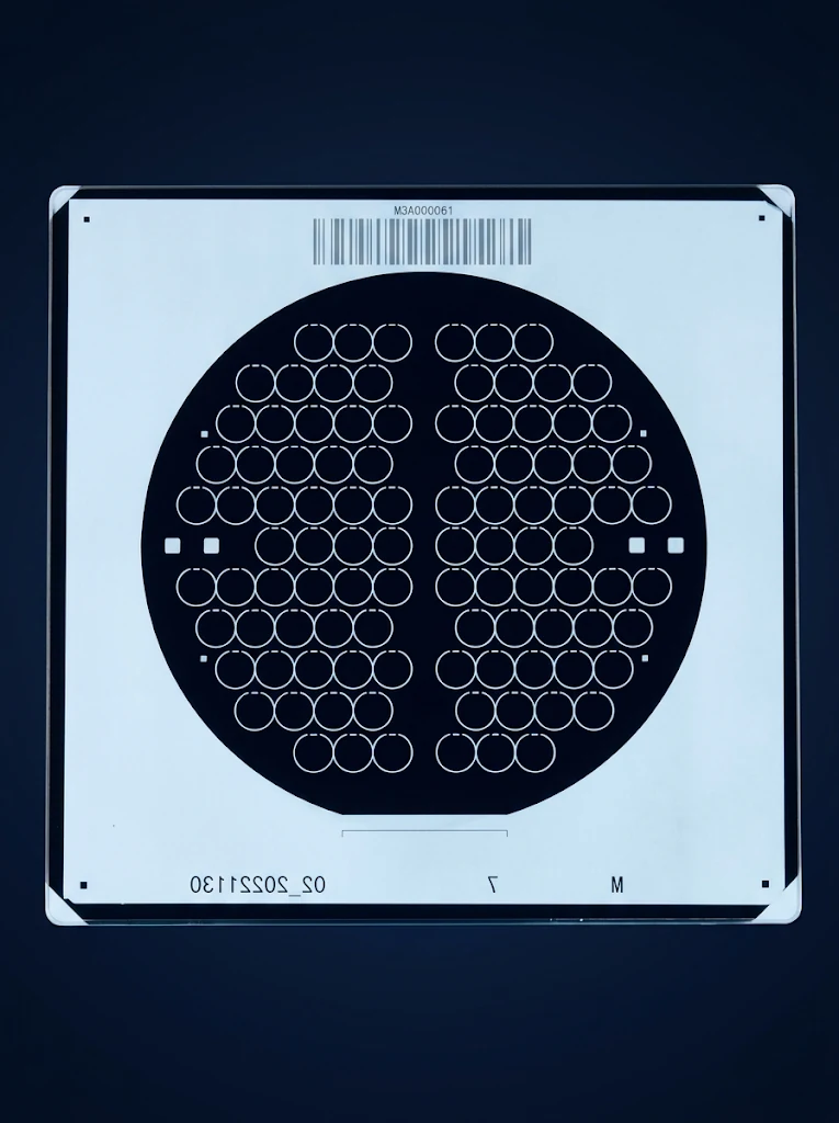
Opaque/clear artwork for a compatible exposure process.
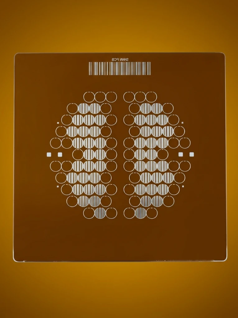
Patterned contact-exposure tooling.
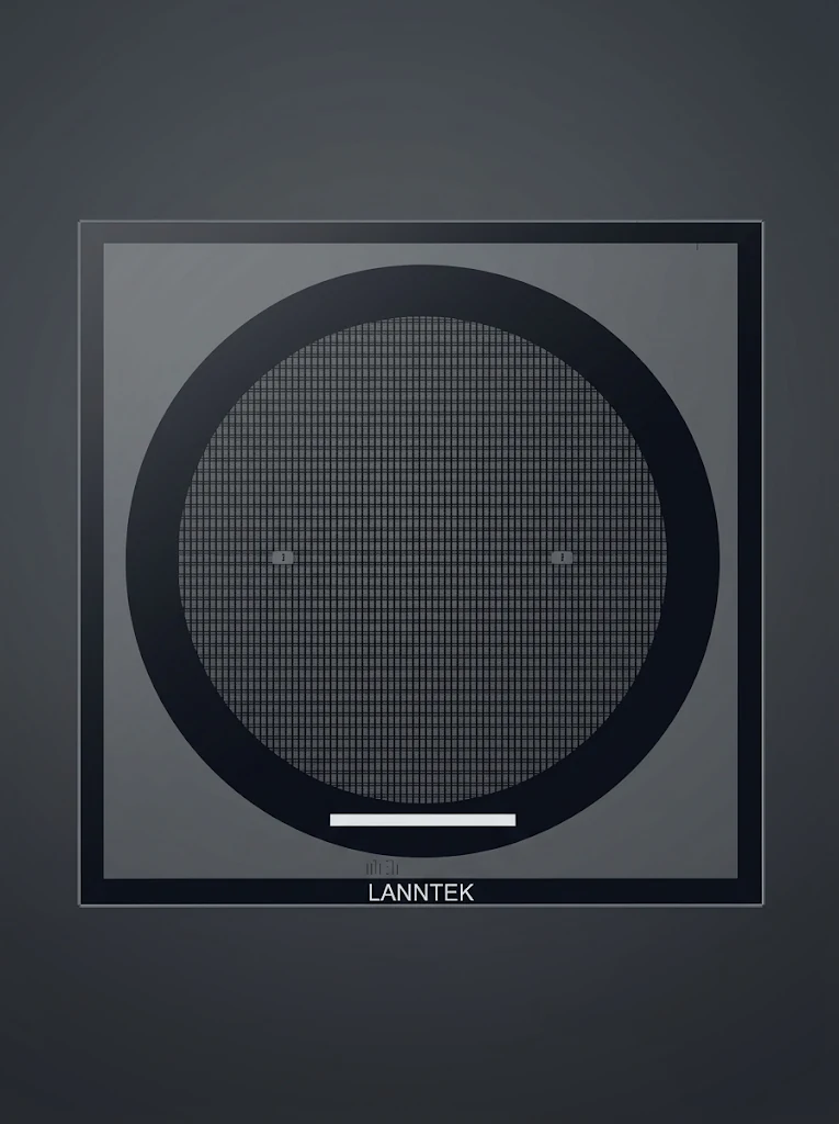
Masks for larger panels and repeated layouts.
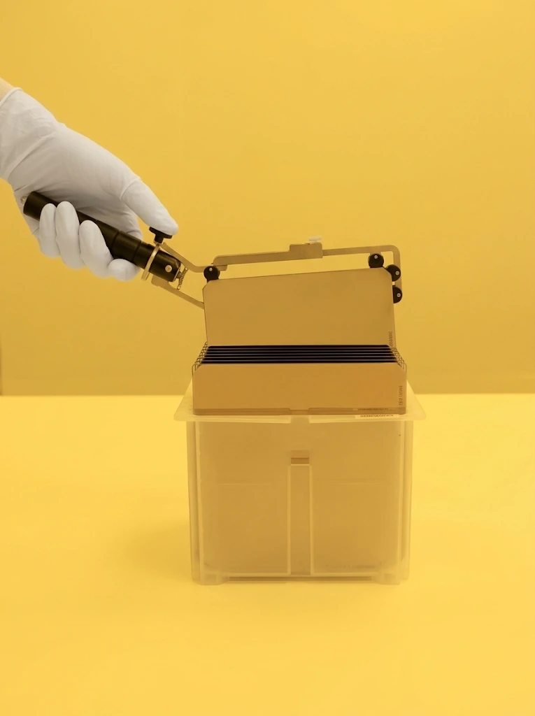
Starting material for making the glass phototool.
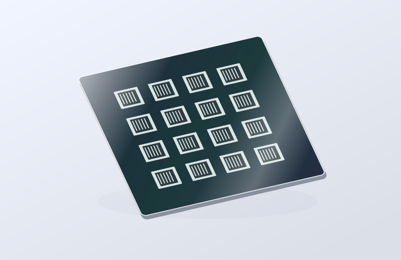
Controlled master artwork for repeat mask production.
A rigid glass phototool carries artwork for a photoimaging process before subsequent material processing. Repeated circuit patterns, alignment features and panel coordinates can be combined in the mask. A coated blank supplies the initial material when phototools are fabricated in-house.
Confirm that the production line uses a mask-based imaging route. Direct imaging onto a circuit panel may not require a physical phototool. Where a mask is used, distinguish mask dimensions from finished conductor dimensions and include any process compensation in the approved artwork.
Circuit artwork must match the resist polarity and the subsequent material-removal or deposition route. Reading side and alignment marks affect how the pattern appears on the workpiece. Distinguish a glass master used for transfer from the final circuit or lead frame.
Mask-based PCB, flexible-circuit and lead-frame processes can use glass artwork tools for circuits, openings and alignment marks.
Confirm whether the line uses physical masks or direct imaging before selecting a mask component.
No. The imaging route determines whether a physical artwork tool is used; direct-imaging processes may not need the same mask.