
Chrome-coated starting material when resist coating follows separately.
Chrome-Coated Photomask Blanks
Chrome-coated glass blanks prepared for photolithographic patterning and custom photomask fabrication.
The foundation for your chrome pattern.
Chrome-coated blanksCustom formats
Product selection
What it is and what it does
Also described as chrome-on-glass blanks, they are supplied before the final pattern transfer step. The blank is defined by the substrate, chromium film, optical density or reflectivity target, surface condition and the photoresist process that will follow.
When to choose it
Choose the supply stage that matches the processes you perform in-house: bare glass before coating, chromium-coated glass before resist coating, or a resist-coated plate before exposure.
How it differs from related products
This blank already has chromium but no final pattern. Choose it rather than a resist-coated plate when you need to select and apply your own resist; choose a finished mask when exposure artwork should already be present.
What can be customised
Material grade, outline, thickness, polished area and edge finish define the substrate. Coated versions also allow a film stack and resist preparation matched to the downstream exposure and etching process.
What you receive
The supplied item is an unpatterned substrate or coated blank in the selected process state. A finished reticle, encoder track or exposure mask requires a subsequent patterning step. Handling, storage and any accompanying inspection data depend on the selected coating and order.
Specifications and inspection
Product configuration
| Product type | Unpatterned chrome-coated photomask blank |
|---|---|
| Substrate | Glass or fused silica, as specified |
| Chrome layer | Sputtered or deposited chromium; thickness to specification |
| Optical behavior | Optical density, reflectivity or contrast target to process |
| Surface | Flatness, surface quality, cleanliness and edge condition |
Small-format blank dimensions
Both substrate surfaces are polished. S = soda-lime glass; WC = white crown glass. Dimensional limits and flatness apply to the individual format and material listed below.
| Format code | Material | Nominal format (in) | Side length (mm) | Thickness (mm) | Flatness (µm) |
|---|---|---|---|---|---|
| 3004 | S | 3 × 3 | 75.4–76.2 | 0.90–1.05 | ≤5 |
| 3006 | S | 3 × 3 | 75.4–76.2 | 1.40–1.60 | ≤5 |
| 3006 | WC | 3 × 3 | 75.4–76.2 | 1.50–1.55 | ≤20 |
| Format code | Material | Nominal format (in) | Side length (mm) | Thickness (mm) | Flatness (µm) |
|---|---|---|---|---|---|
| 4004 | S | 4 × 4 | 100.8–101.6 | 0.90–1.05 | ≤5 |
| 4004 | WC | 4 × 4 | 100.95–101.45 | 0.97–1.03 | ≤20 |
| 4006 | S | 4 × 4 | 100.8–101.6 | 1.40–1.55 | ≤5 |
| 4006 | WC | 4 × 4 | 100.8–101.6 | 1.45–1.55 | ≤20 |
| 4008 | S | 4 × 4 | 100.8–101.6 | 1.95–2.05 | ≤5 |
| 4008 | WC | 4 × 4 | 100.8–101.6 | 2.00–2.05 | ≤20 |
| 4009 | S | 4 × 4 | 100.8–101.6 | 2.20–2.40 | ≤5 |
| 4009 | WC | 4 × 4 | 100.8–101.6 | 2.30–2.40 | ≤5 |
| 4010 | S | 4 × 4 | 100.8–101.6 | 2.44–2.64 | ≤5 |
| 4010 | WC | 4 × 4 | 100.8–101.6 | 2.50–2.60 | ≤20 |
| 4012 | S | 4 × 4 | 100.8–101.6 | 2.95–3.05 | ≤5 |
| 4012 | WC | 4 × 4 | 100.8–101.6 | 2.95–3.00 | ≤20 |
| 4016 | WC | 4 × 4 | 100.8–101.6 | 4.00–4.05 | ≤20 |
| 4018 | WC | 4 × 4 | 100.8–101.6 | 4.50–4.55 | ≤20 |
| 4020 | WC | 4 × 4 | 101.2–101.4 | 4.90–5.00 | ≤20 |
| Format code | Material | Nominal format (in) | Side length (mm) | Thickness (mm) | Flatness (µm) |
|---|---|---|---|---|---|
| 5002 | S | 5 × 5 | 126.2–127.0 | 0.45–0.55 | ≤20 |
| 5002 | WC | 5 × 5 | 126.2–127.0 | 0.45–0.55 | ≤20 |
| 5004 | S | 5 × 5 | 126.2–127.0 | 0.95–1.05 | ≤20 |
| 5004 | WC | 5 × 5 | 126.2–127.0 | 0.95–1.05 | ≤20 |
| 5006 | WC | 5 × 5 | 126.2–127.0 | 1.45–1.55 | ≤20 |
| 5008 | WC | 5 × 5 | 126.2–127.0 | 2.00–2.05 | ≤20 |
| 5009 | S | 5 × 5 | 126.2–127.0 | 2.20–2.40 | ≤8 |
| 5012 | WC | 5 × 5 | 126.2–127.0 | 2.95–3.05 | ≤20 |
| 5014 | WC | 5 × 5 | 126.2–127.0 | 3.45–3.55 | ≤20 |
| Format code | Material | Nominal format (in) | Side length (mm) | Thickness (mm) | Flatness (µm) |
|---|---|---|---|---|---|
| 6009 | S | 6 × 6 | 151.6–152.4 | 2.20–2.40 | ≤10 |
| 6009 | WC | 6 × 6 | 151.75–152.25 | 2.30–2.40 | ≤20 |
| 6012 | S | 6 × 6 | 151.6–152.4 | 2.95–3.15 | ≤10 |
| 6023 | S | 6 × 6 | 151.6–152.4 | 5.75–5.95 | ≤10 |
| 6025 | S | 6 × 6 | 151.6–152.4 | 6.25–6.45 | ≤10 |
| Format code | Material | Nominal format (in) | Side length (mm) | Thickness (mm) | Flatness (µm) |
|---|---|---|---|---|---|
| 7009 | S | 7 × 7 | 177.0–177.8 | 2.20–2.40 | ≤15 |
| 7012 | S | 7 × 7 | 177.0–177.8 | 2.95–3.15 | ≤15 |
| 7012 | WC | 7 × 7 | 177.0–177.8 | 2.95–3.15 | ≤30 |
Chromium film specifications
Select the film type by optical density, reflectance and pattern-transfer requirements. LRC = low-reflective chrome; HRC = high-reflective chrome; BCB = blue-chrome-blue. Film thickness is expressed in nm (1 nm = 10 Å).
| Film type | Coating family | Film thickness (nm) | Optical density / wavelength | Reflectance / wavelength | Wet etch time (s) |
|---|---|---|---|---|---|
| Type-1 | LRC | 100 ± 8 | 3.1 ± 0.2 @ 450 nm | 11 ± 2% @ 436 nm | 43–53 |
| Type-2 | LRC | 125 ± 10 | 4.0 ± 0.2 @ 450 nm | 11 ± 2% @ 436 nm | 50–60 |
| Type-3 | BCB | 200 ± 20 | 5.0 ± 0.3 @ 450 nm | ≤7% @ 600 ± 50 nm | >70 |
| Type-4 | LRC | 200 ± 20 | 5.0 ± 0.3 @ 450 nm | 11 ± 2% @ 436 nm | >70 |
| Type-5 | HRC | 100 ± 10 | 3.1 ± 0.2 @ 550 nm | ≥45% @ 436 nm | 43–53 |
| Type-6 | BCB | 250 ± 20 | 5.0 ± 0.3 @ 500 nm | ≤7% @ 600 ± 50 nm | >70 |
| Type-7 | LRC | 125 ± 10 | 3.1 ± 0.2 @ 550 nm | 11 ± 2% @ 436 nm | 50–60 |
| Type-8 | HRC | 200 ± 20 | 5.0 ± 0.3 @ 550 nm | ≥45% @ 436 nm | >70 |
Wet etch times are measured by immersion with stirring at 20 ± 0.1 °C, using 200 g ceric ammonium nitrate and 35 mL glacial acetic acid, with deionized water to a total volume of 1000 mL. The bilateral undercut rate is <0.07 µm per 10 s, excluding BCB.
| Coating family | 98% H₂SO₄ at 120 °C | 98% H₂SO₄ + H₂O₂ at 75 °C |
|---|---|---|
| LRC / HRC | >120 min | >120 min |
| BCB | >60 min | >60 min |
Optical properties are measured on one witness sample per lot. Film thickness is measured by step profilometry; optical density by densitometry; reflectance by spectrophotometry.
Chrome-coated photomask blanks combine a polished glass substrate with a deposited chromium film for subsequent photolithographic patterning.
Built for your process.
Request a Quote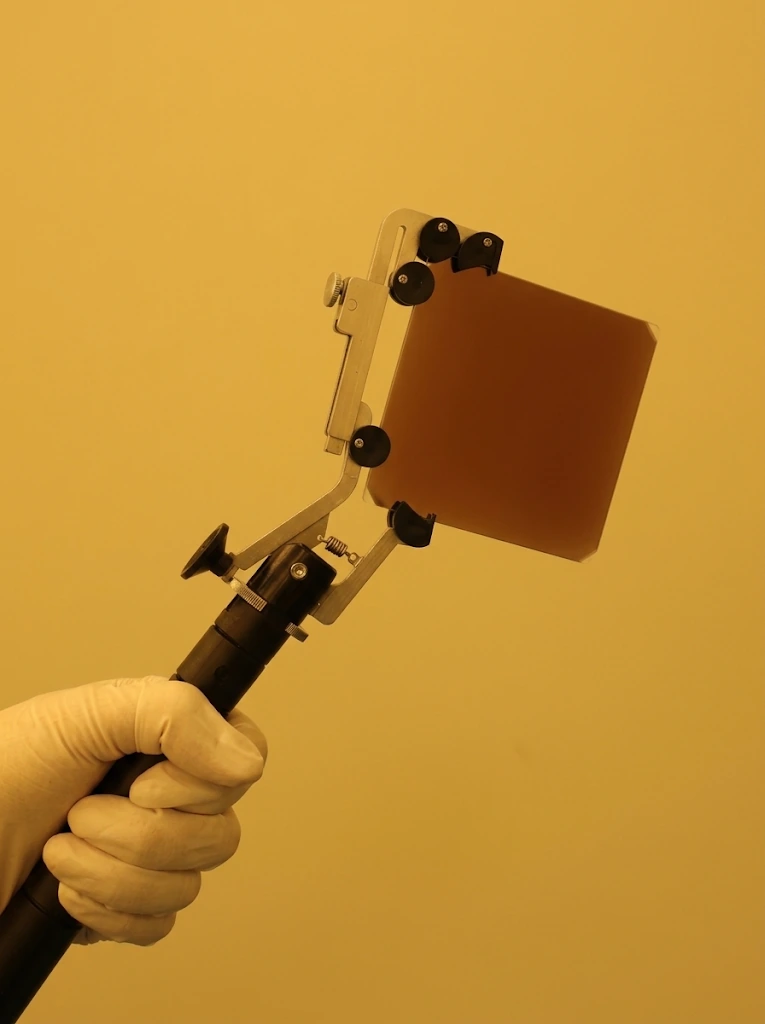
Where it fits in the process
Choose a chrome-coated blank when the final pattern will be formed in a chromium film by laser writing, exposure and etching.
Substrate finish and defect limits
| Property | Specification |
|---|---|
| Squareness | 90° ± 5′ |
| Edge chamfer | 45° |
| Bevel width, thickness ≤1.6 mm | 0.20–0.50 mm |
| Bevel width, thickness >1.6 mm | 0.40–0.80 mm |
| Corner radius | 2.00–3.00 mm |
| Effective inspection area | Square side D = L − 12.7 mm, where L is the plate side length. |
| Defect | Acceptance limit |
|---|---|
| Cracks / chips | No defects >2 mm in the effective area |
| Bubbles / inclusions | No defects >5 µm |
| Pits | No defects >5 µm |
| Scratches | Limit: 5 µm × 1 mm in the effective area |
Glass appearance inspection uses a 120,000 lux halogen inspection lamp at a distance of 15 cm from the substrate.
| Grade | Pinhole size | Acceptance limit |
|---|---|---|
| High Grade | <2 µm | No limit |
| High Grade | 2–5 µm | ≤0.3 / in² |
| High Grade | >5 µm | None permitted |
| Standard Grade | >2 µm | ≤0.5 / in² |
| Standard Grade | >5 µm | None permitted |
| BCB | >5 µm | ≤0.5 / in² |
| BCB | >10 µm | None permitted |
Every plate undergoes pinhole inspection. Defect density and the no-defect size limit both apply to the selected grade.
Low-reflectance chromium: optical and process properties
Low-reflectance chromium (LRC), blue chromium coatings and high-reflectance chromium (HRC) serve different optical roles. Select optical density and reflectance at the operating wavelength; a blue appearance alone does not specify optical performance.
| Property | Measurement condition | Specification |
|---|---|---|
| Film thickness | Nominal 100 nm coating | 100 ±8 nm |
| Optical density | 450 nm | 3.1 ±0.2 |
| Reflectance | 436 nm | 11 ±2% |
| Sheet resistance | Four-point probe | <26 Ω/□ |
| Wet etch time | Manual test method | 53 ±5 s |
| Lateral undercut | APT test designation | <0.07 µm / 10 s |
| Chemical resistance | Concentrated H₂SO₄ at 120 °C | >120 min |
| Chemical resistance | Concentrated H₂SO₄ + H₂O₂ at 120 °C | >120 min |
This is a separate LRC process specification. The manual 53 ±5 s etch result is distinct from the stirred-immersion film-type schedule. The 120 °C peroxide-mixture condition is also distinct from the 75 °C coating-family test. Specify the selected method and coating configuration on the order.
Etch-rate comparison requires the same bath composition, temperature, agitation and endpoint definition. The APT designation must be defined in the test procedure before its undercut value is compared with a different measurement method.
Reflectance is wavelength dependent. The 436 nm value is the specified inspection point; it is not a constant across the visible spectrum. For another operating wavelength, include the required reflectance and measurement side in your inquiry.
Chromium-film pinhole grades by substrate format
A pinhole in this specification is an unintended transparent defect in the chromium film. It is not a designed optical aperture and does not indicate a hole through the glass. Select the format and coating acceptance grade together.
| Acceptance grade | Rejected pinhole sizes |
|---|---|
| Standard Grade | d ≥5 µm |
| Premium Grade | d ≥1 µm |
These thresholds define the rejected defect sizes. The inspection specification must also define any permitted defect count below the threshold and the inspected area.
| Acceptance grade | Defect size, d | Acceptance limit |
|---|---|---|
| A | 5 ≤ d < 10 µm | ≤0.01 / cm² |
| A | d ≥ 10 µm | None permitted |
| B | 5 ≤ d < 10 µm | ≤0.01 / cm² |
| B | 10 ≤ d < 30 µm | ≤0.003 / cm² |
| B | d ≥ 30 µm | None permitted |
| C | 5 ≤ d < 10 µm | ≤0.01 / cm² |
| C | 10 ≤ d < 50 µm | ≤0.003 / cm² |
| C | d ≥ 50 µm | None permitted |
The no-defect threshold takes precedence at the boundary of each size band. For example, Grade B rejects all pinholes of 30 µm or larger. Specify inspected area, edge exclusions and the count-rounding rule for area-based density limits. No acceptance value is assigned here to pinholes smaller than 5 µm.
Large-format glass substrates
Large-format substrate flatness is specified by plate dimensions and thickness. Use these limits for the listed large-format configurations rather than applying a small precision-substrate flatness value to every plate size.
| Thickness (mm) | Plate-dimension range (mm) | Maximum flatness (µm) |
|---|---|---|
| 3.0 / 4.8 | 228.6 × 228.6 to 508 × 609.6 | ≤70 |
| 3.0 / 4.8 | 609.6 × 609.6 to 700 × 800 | ≤100 |
| 7.8 | 620 × 720 to 700 × 800 | ≤120 |
Specify the required plate dimensions within the listed format ranges, the support condition, measurement area and inspection orientation. The supplied specification should identify whether flatness is assessed before or after coating.
What can be customized
- Substrate material, size and thickness
- Chrome thickness, optical density and reflectivity
- Photoresist compatibility and coating condition
- Inspection, cleaning and protective packaging
Where this product is used
Common questions
What is a chrome-coated photomask blank?
It is an unpatterned glass or fused silica substrate with a chromium film, supplied for a later patterning process.
Does the blank include a photoresist layer?
It can be supplied with or without photoresist, depending on the required process route.
Can the chrome layer be made for laser writing?
Yes. The coating and resist route should be specified around the laser direct-write process.
Selection notes
Chrome-coated photomask blanks are polished substrates with an unpatterned chromium film for subsequent pattern fabrication.
Match the substrate and plate format to the chromium stack, optical density, defect grade and any required photoresist coating.
Information for your inquiry
Substrate, plate dimensions, chromium and optical requirements, downstream resist process, defect grade and quantity.
Does a chrome blank already contain my pattern?
No. A blank provides a uniform film. Compatible resist coating, exposure, development and etching create the pattern. Supply artwork when ordering a finished patterned component.