
Chrome-Coated Photomask Blanks: Flatness and Defect Grades
A blank is not specified by a grade. Four independent acceptance sets decide whether it survives your process — and two of them change meaning depending on how the plate is held and whether it was measured before or after coating.
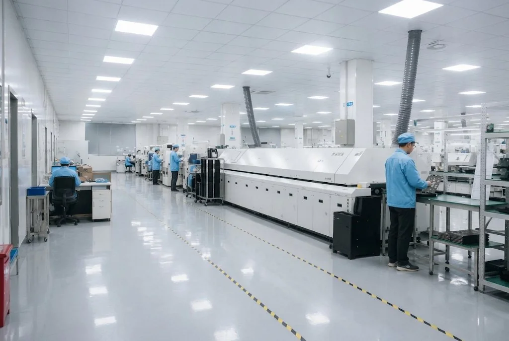
What you are buying, before you buy it
Ordering a blank by grade fixes one of four acceptance sets and leaves three open. The two that cause the most rework are flatness — which is only valid together with a support condition and a measurement area — and the defect schedule, which does not cover the film at all.
A chrome-coated photomask blank is a polished substrate carrying an unpatterned chromium-based film. It is bought before the resist step and well before any exposure, which is why the same glass appears under several product names that are not interchangeable. The four supply states below differ in what has already been accepted and what is still open.
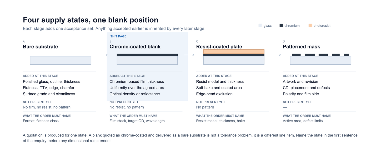
Entering an enquiry at the wrong state is the cheapest mistake to avoid and the most expensive to discover. A blank quoted as "chrome-coated" and delivered without resist stops a line; a resist-coated plate ordered for a process that coats in-house adds a shelf-life problem nobody asked for. Start the enquiry with the state, then the dimensions.
What follows the blank also constrains it. The photolithography route runs from substrate preparation through sputtering, resist coating, soft bake, exposure, development, chrome etch, stripping and final inspection. Each of those steps reads something different from the blank: the writer reads flatness and reflectance, the resist reads surface energy and cleanliness, the etch reads film chemistry and thickness.
The four acceptance sets behind one grade
A purchase order usually says something like "Grade A, 6 inch, chrome blank". That sentence fixes one axis — the substrate defect schedule — and leaves the other three to be decided by whoever writes the process sheet. They are not ranked against each other, and improving one does not improve another.
| Acceptance set | What is measured | Published values | What the drawing must add |
|---|---|---|---|
| Substrate geometry | Outline, thickness, total thickness variation, flatness, edge condition | Formats 3–9 in; thickness ≥0.3 mm; TTV ≤2 µm; flatness ≤2 µm or the format-code limit; 45° chamfer; |A−B| <5 µm; edge squareness <0.015 in per 1 in | Support condition, measurement area, whether flatness is assessed before or after coating, and the test method |
| Substrate defects | Bubbles, surface pits, inclusions, cracks and chips in the glass | Grade A and Grade C schedules, with size bands and permitted counts per inspection area | The inspection area, the excluded border, the grade, and any defect type the chosen schedule does not address |
| Film | Thickness, uniformity, optical density or reflectance, adhesion | 10–1,000 nm multilayer development with ±1% uniformity over the agreed measurement area; 0.1–20 µm functional layers; Cr, Cr oxide, Cr nitride, Al, Al-Cu, Ag, Au, ITO, AZO and AR dielectric families | Target thickness and tolerance, the wavelength for density or reflectance, the uniformity measurement area, and any abrasion requirement |
| Surface condition | Particles, stains, residue, protective packaging | Polished surfaces supplied to Grade 0 appearance requirements; cleaning and packaging agreed per order | Particle size and area limits, permitted cleaning agents, and the packaging and handling agreed for the route |
The four sets interact in one direction only: a defect accepted in an earlier set is inherited by everything built on it. A bubble inside the inspection area cannot be coated away, and a film cannot be inspected for pinholes until its substrate has passed. That is the practical argument for releasing the blank on a drawing that names all four, rather than on a grade word that names one.
Format and flatness: two schedules, one outline
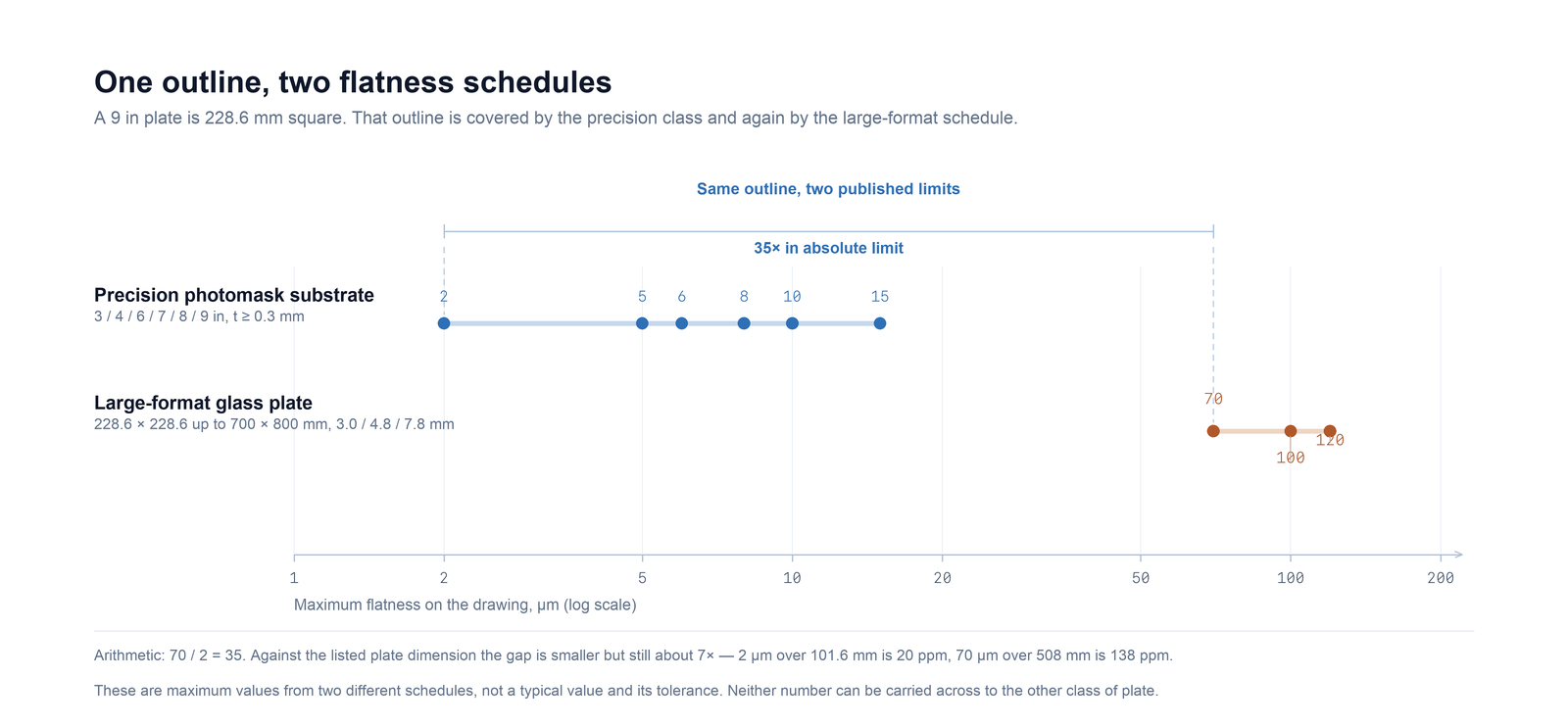
The precision substrate class covers 3, 4, 6, 7, 8 and 9 in squares at 0.3 mm and above, with total thickness variation at 2 µm or better and flatness at 2 µm. Below that headline figure the format codes carry a set of selectable flatness limits: fused-silica formats are listed at 2, 5, 6 or 10 µm, and soda-lime formats at 5, 8, 10 or 15 µm depending on the code.
Separately, the site publishes a flatness schedule for large glass plates: 70 µm for 3.0 and 4.8 mm plates between 228.6 × 228.6 mm and 508 × 609.6 mm, 100 µm between 609.6 × 609.6 mm and 700 × 800 mm, and 120 µm for 7.8 mm plates from 620 × 720 mm to 700 × 800 mm. The first entry starts at 228.6 mm, which is 9 in: an outline that the precision class also covers, at 2 µm.
| Property | Precision photomask substrate | Large-format glass plate |
|---|---|---|
| Outline | 3 / 4 / 6 / 7 / 8 / 9 in square | 228.6 × 228.6 to 700 × 800 mm |
| Thickness | ≥0.3 mm, as specified | 3.0 / 4.8 / 7.8 mm |
| Maximum flatness | ≤2 µm, or the format-code limit (2–15 µm) | ≤70 / 100 / 120 µm by size and thickness |
| Total thickness variation | ≤2 µm | Confirm with supplier for the plate |
| Typical use | Masks, reticles, scales, targets | Large plates for display-scale work |
Neither number is wrong. The schedules describe different plates: a 3.0 mm plate spanning 700 mm has an aspect ratio of about 233:1, and stiffness falls with the cube of thickness, so the same absolute flatness is not physically available across that span. What matters commercially is that the quotation names the schedule it used.
Flatness is conditional, and so is thickness
Three quantities are routinely written as if they were one. Flatness is the deviation of a surface from a plane, evaluated with tilt removed. Total thickness variation is how the thickness changes across the plate. The face-to-face difference |A−B| compares thickness at two specified positions. They answer different questions, and only the first is a surface measurement.
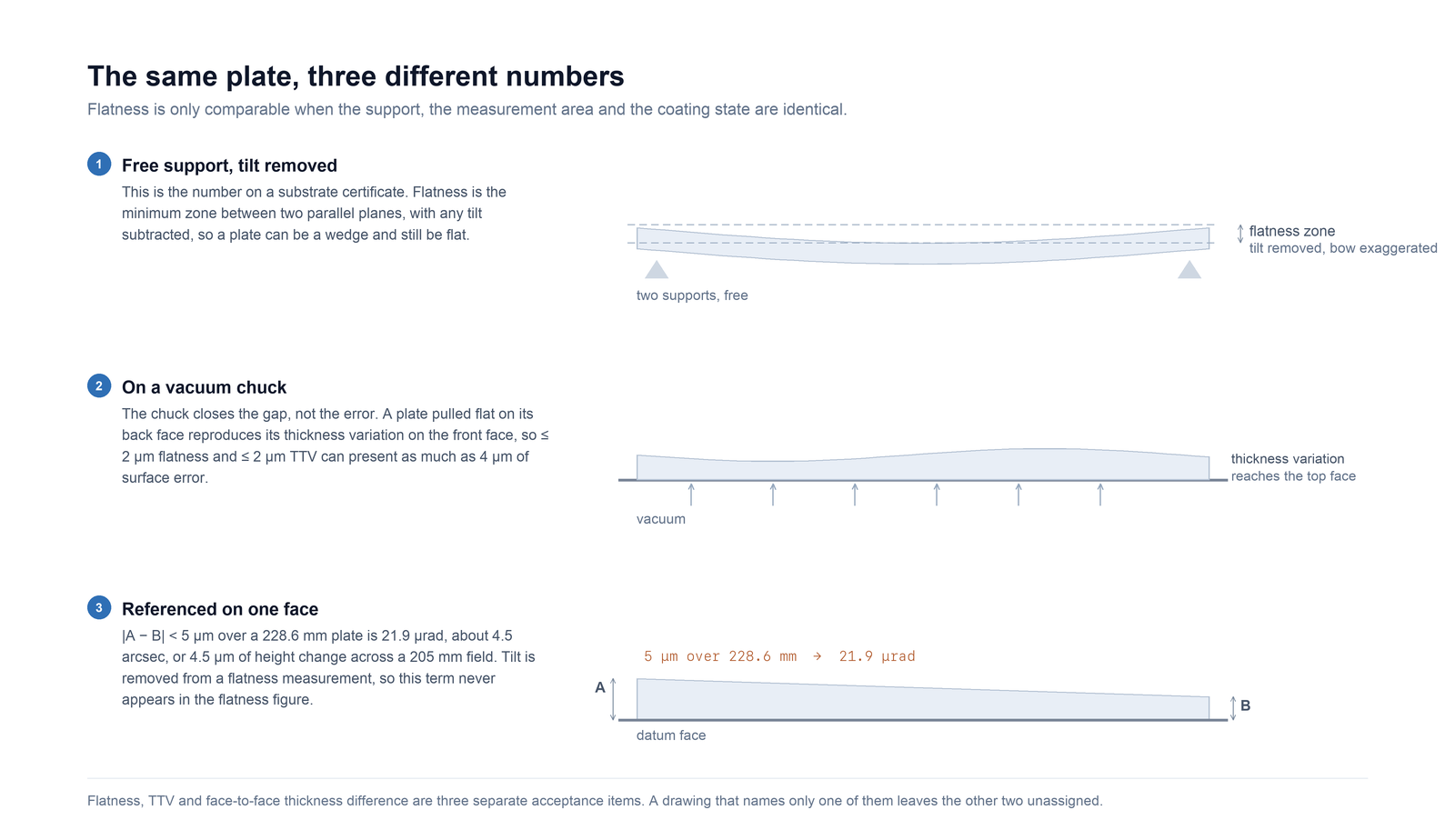
Tilt is removed; thickness is not
Because a flatness evaluation subtracts tilt, a plate can be an excellent flatness result and a poor parallel plate at the same time. That is not a defect in either specification; it is a reason to write both. The published precision figures put flatness at 2 µm and |A−B| below 5 µm: two independent limits, measured in two different ways, on the same part.
On a chuck, the two limits meet
Most exposure and inspection fixtures hold a plate by vacuum against a flat reference. The chuck removes the gap between the plate and the reference; it does not remove the error. A plate flattened on its back face reproduces its thickness variation on its front face, so a part accepted at 2 µm flatness and 2 µm TTV can present up to 4 µm of surface error in the fixture. That sum is arithmetic, not statistics, and it is the reason a TTV line belongs on a blank drawing whenever the plate will be chucked.
Before or after coating
A sputtered film changes the stress state of a thin plate, so the flatness of a coated blank is not automatically the flatness of the substrate it was made from. The published substrate guidance is explicit that the supplied specification should identify whether flatness is assessed before or after coating, and whether the measurement covers the full plate or only the clear aperture. Both answers are legitimate; an unstated answer is not.
A flatness figure has meaning only together with a measurement area, a support condition and a test method. Two plates with the same certificate can differ by a factor of two in the fixture if one was measured over the full plate on three points and the other over the central 90% on a chuck.
The film: what the next process asks of it
The coating stage develops 10–1,000 nm micro-nano films and multilayer stacks, with uniformity targeted to ±1% over the agreed measurement area, and 0.1–20 µm functional layers where a thicker layer is needed. The available families include chromium, chromium oxide and chromium nitride, aluminium and Al-Cu alloys, silver and gold, IR-transmissive ITO and AZO, and AR dielectric multilayers. The film is specified for a process, not chosen from a list.
Optical density is the value that most often arrives underspecified. Density is a logarithmic transmission figure at a stated wavelength, so density 3 corresponds to 0.1% transmission and density 5 to 0.001% — a hundredfold difference that both look like "opaque" on a bench. Without the wavelength, the number does not identify a film.
| Next process | What the film has to do | State on the drawing |
|---|---|---|
| Contact exposure | Survive repeated contact with resist-coated workpieces without damage that shows up in the pattern | Film chemistry and thickness, plus any abrasion requirement you will test to |
| Proximity exposure | Give a defined edge at the exposure wavelength while the plate sets the gap | Density at the exposure wavelength, thickness tolerance, flatness class and gap |
| Laser direct writing | Provide the density and reflectance the writer's focus and inspection need, and accept the resist that follows | Density or reflectance at the write wavelength, film thickness, resist compatibility |
| Backside alignment | Transmit enough at the alignment wavelength through substrate and film together | Transmission or density at the alignment wavelength, substrate material and thickness |
| Etch and strip | Etch consistently across the plate and survive the stripper without lifting | Film chemistry, thickness, adhesion requirement, permitted process chemistry |
Defect acceptance: two schedules, one gap
The substrate schedules are published as size bands with permitted counts, and the counts refer to the agreed inspection area rather than to a density per square centimetre. That distinction matters: three bubbles below 10 µm are three in the whole inspected area, whatever its size, so the inspection area is a commercial term and not a formality.
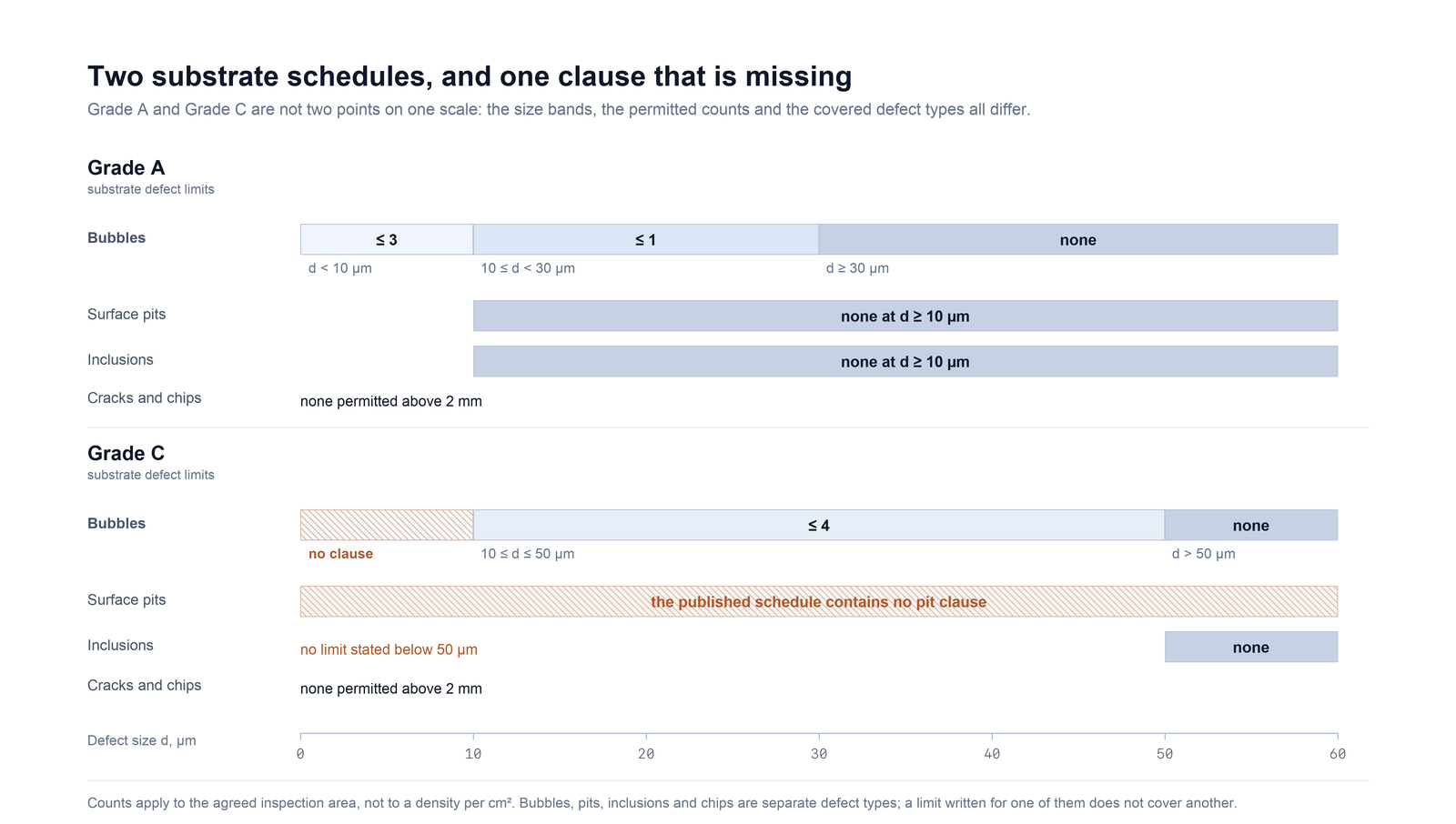
Grade A and Grade C are not two points on a single scale. Grade A permits up to three bubbles below 10 µm, one between 10 and 30 µm and none at 30 µm or above, and forbids surface pits and inclusions at 10 µm and above. Grade C states no limit for bubbles below 10 µm, permits four between 10 and 50 µm, forbids bubbles above 50 µm, and forbids inclusions only at 50 µm and above. Both forbid cracks and chips above 2 mm.
Read side by side, three things follow. Grade C is not simply a looser Grade A: it is silent below 10 µm, which is not the same as permitting defects there. Its inclusion threshold is five times larger. And the published Grade C schedule contains no surface-pit clause at all, so a pit requirement has to be written into the drawing rather than inferred from the grade. If pits matter to your process — they usually do when the film is thin or the plate is used in transmission — that is the clause to check first.
None of these schedules covers the film. Pinholes, coating inclusions and edge-coating defects are a separate inspection with separate limits. For a blank, the film acceptance is agreed against the drawing's active area.
The drawing and the RFQ
A complete blank enquiry is short, but it is complete on all four acceptance sets. The right-hand column is the one that produces a second round of questions.
| Item | A complete line looks like | Commonly left out |
|---|---|---|
| Supply state | Chrome-coated blank, no resist; or chrome plus resist with model and thickness | Whether resist will be applied in-house |
| Substrate | Material grade, outline, thickness | The glass grade, when only "glass" is written |
| Flatness | Limit, class, measurement area, support condition | Measurement area and support |
| Coating state | Whether flatness is assessed before or after coating | The state the figure refers to |
| Thickness variation | TTV and |A−B|, if the plate will be chucked or gap-referenced | |A−B|, when only flatness is given |
| Edge | Chamfer, squareness, any chip limit at the edge | Edge condition entirely |
| Defect grade | Grade, inspection area, excluded border, any defect type outside the schedule | The inspection area |
| Film | Stack, thickness and tolerance, uniformity and its measurement area | The uniformity measurement area |
| Optical target | Density or reflectance value with the wavelength | The wavelength |
| Cleanliness and packaging | Particle limit, permitted cleaning, packaging and handling | Packaging, until after the first damaged delivery |
| Records | Which measurements are reported, by which method | The method, when a certificate is requested |
Inspection and acceptance
Inspection of a blank checks four things in this order: the substrate geometry against the drawing, the substrate defects against the selected grade and inspection area, the film against its thickness, uniformity and optical target, and the surface against the agreed cleanliness and packaging conditions. A dimensional record and an optical record answer different questions.
Two limits on that inspection are worth stating plainly. A certificate reports the measurements named in the order; it does not silently extend to quantities nobody asked for. And acceptance of a blank says nothing about the pattern that will be written on it — the finished mask is accepted against its own drawing, where the published line-width tolerance is ±0.2 µm.
Common questions
Is a higher substrate grade always the safer choice for a blank?
Not on its own. The substrate defect grade covers bubbles, pits, inclusions and chips in the glass. It says nothing about the film, the cleanliness of the coated surface or the flatness of the plate in the holder. A Grade A substrate with an uncontrolled film is not a better blank than a Grade C substrate with a specified film, because the two parts of the order are accepted against different schedules.
Can the same 9 in plate be quoted at 2 µm and at 70 µm flatness?
Yes, because the two numbers come from different schedules. The precision photomask substrate class lists flatness at 2 µm for 3 to 9 in formats. The large-format plate schedule lists 70 µm for 3.0 and 4.8 mm plates from 228.6 mm square upwards, and 228.6 mm is 9 in. The schedule that applies depends on the class of plate and on the process it feeds, and it should be named in the quotation.
Does a flatness limit of 2 µm include thickness variation?
No. Flatness describes the deviation of one surface from a plane, with tilt removed. Total thickness variation describes how the thickness changes across the plate. They are separate limits and they are not additive in a budget, but they combine on the part: a plate pulled flat against a chuck presents its thickness variation on the working surface. Name both on the drawing.
Is chrome thickness the same as optical density?
No. Optical density is a logarithmic transmission value at a stated wavelength, so it depends on the film material and on how that material behaves at that wavelength, not on thickness alone. A thickness figure without a wavelength and a measurement method does not fix the density you will get. State the density or the reflectance you need, at the wavelength you will use.
Can the blank be supplied with the resist already applied?
Yes. Resist coating is the next supply state, and the resist model, thickness, coated area and edge-bead exclusion are then part of the same order. Once resist is present, shelf life, storage conditions and the soft-bake state also become part of the specification, so they are usually discussed together with the coating step rather than with the blank.
What do the substrate defect grades not cover?
They cover defects in the glass. They do not cover pinholes or other defects in the chromium film, particles or residue on the coated surface, or stains from handling and packaging, which are inspected separately. The published schedules also differ in scope: Grade A states a limit for surface pits and Grade C does not, so a defect type that matters to your process may need to be written into the drawing rather than inferred from the grade.
Send the outline, the schedule and the process that follows
Quotations for blanks move fastest when the four acceptance sets arrive together. If one of them is still open, say which one — we can quote the options rather than guess.