
How much optical density does a photomask actually need?
Optical density on a photomask is set by the dose that leaks into a dark area, not by contrast. How to calculate the OD you need, and where measurement stops.
The short answer
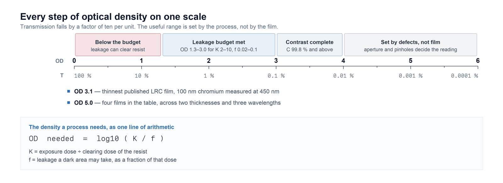
Optical density is not an opacity rating. It is one number from a division: how many times over the resist's clearing dose you expose, divided by the fraction of that dose you are willing to let through a dark area. OD = log10(K ÷ f).
A normal positive-tone contact or proximity process lands between 1.3 and 3.0 — below the 3.1 of the thinnest film in the catalogue. Above about OD 4 the figure stops describing the film and starts describing how you measured it.
One number, one division
Optical density is a logarithmic transmission figure at a stated wavelength: OD = −log10(T), where T is the fraction of light that gets through. Density 3 is 0.1 % transmission, density 5 is 0.001 %. Two other pages here already define the term and warn that it does not describe reflectance, pinholes or edge quality — the patterned glass materials guide and the chrome-coated blank guide. Neither answers the question a drawing actually asks: which number.
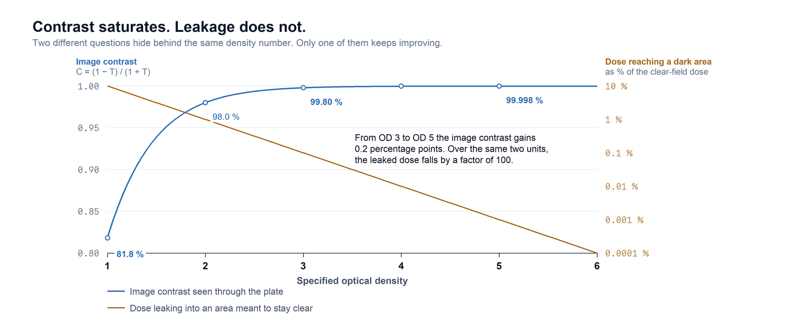
The reason the question is hard is that the same figure answers two unrelated things at once. It sets how much light reaches the resist where the mask is meant to be opaque, and it sets how much light the film returns to an inspection camera. The first is an exposure question with an arithmetic answer. The second is a contrast question that stops improving early. Table 1 puts both on the same scale, together with the measurement limit that sits underneath them.
| Density | Transmission | Dose into a dark area | Image contrast C | Pinhole, 1 mm² |
|---|---|---|---|---|
| 1.0 | 10 % | 10 | 0.818 | 357 µm |
| 1.5 | 3.16 % | 3.16 | 0.939 | 201 µm |
| 2.0 | 1.00 % | 1.00 | 0.980 | 113 µm |
| 2.5 | 0.316 % | 0.316 | 0.994 | 63.5 µm |
| 3.0 | 0.100 % | 0.100 | 0.998 | 35.7 µm |
| 3.1 | 0.079 % | 0.079 | 0.998 | 31.8 µm |
| 3.5 | 0.032 % | 0.032 | 0.999 | 20.1 µm |
| 4.0 | 0.0100 % | 0.010 | 0.9998 | 11.3 µm |
| 5.0 | 0.00100 % | 0.001 | 0.99998 | 3.57 µm |
| 6.0 | 0.000100 % | 0.0001 | 0.999998 | 1.13 µm |
Read the first three columns and the table looks like an argument for more density. Read the third and fourth together and it stops being one: at OD 3 the image contrast is already 99.8 %, and the three units from OD 3 to OD 6 buy 0.2 percentage points between them. What they do keep buying is a lower leakage dose — which matters only if you can say what the leakage is leaking into.
The density your exposure needs
In a contact or proximity exposure, the clear areas receive the full dose D. The dark areas receive D × T, and a positive-tone resist clears wherever the delivered dose reaches its clearing dose E0. If the leakage reaches that threshold, the area you intended to keep is developed away and the pattern is gone. The requirement is therefore not "be opaque" but "stay below the clearing dose by the margin your process needs".
Let K = D ÷ E0, the factor by which you overexpose to get a usable sidewall, and f the fraction of E0 you allow to leak. Then T ≤ f ÷ K, and the minimum density is log10(K ÷ f).
Both inputs are measurable on your own process, and neither is a property of the mask. That is the whole point: the same mask can be adequate for one exposure and marginal for another, and the difference is K.
| Overexposure K | f = 0.10 | f = 0.05 | f = 0.02 | f = 0.01 |
|---|---|---|---|---|
| 1.5× | 1.18 | 1.48 | 1.88 | 2.18 |
| 2× | 1.30 | 1.60 | 2.00 | 2.30 |
| 3× | 1.48 | 1.78 | 2.18 | 2.48 |
| 5× | 1.70 | 2.00 | 2.40 | 2.70 |
| 10× | 2.00 | 2.30 | 2.70 | 3.00 |
| 30× | 2.48 | 2.78 | 3.18 | 3.48 |
| 100× | 3.00 | 3.30 | 3.70 | 4.00 |
Three worked cases make the range concrete. Take an exposure at 120 mJ/cm² on a resist whose clearing dose is 40 mJ/cm², so K = 3, and allow 5 % of the clearing dose to leak: the minimum is log10(60) = 1.78. A 100 nm LRC film at 3.1 clears that by a factor of 21 in transmission. Push to a thick resist at 600 mJ/cm² on the same 40 mJ/cm² clearing dose, with only 2 % leakage allowed: K = 15, the minimum is log10(750) = 2.88, and the same film still covers it.
To reach OD 5 you need K ÷ f = 100 000. That is not a lithography condition — it is what you get if you overexpose 100× and permit a leakage of one part in a thousand of the clearing dose. Nobody measures the clearing dose that precisely. So when a drawing says OD 5, the number did not come from the resist.
Above OD 4, the resist is no longer the reason
If the exposure budget is satisfied somewhere between 1.3 and 3.0, a specification of 4 or 5 is carrying a different requirement. It is worth naming which one, because the four candidates are measured in four different places — and only one of them is measured on the plate you are buying.
| Mechanism | The quantity that actually has to be met | Where it is verified |
|---|---|---|
| Resist clearing in a dark field | Leakage dose against the clearing dose of your resist, at your exposure wavelength | Your own test exposure, on your coater and developer |
| Inspection or machine-vision contrast | Image contrast through the plate, C = (1 − T) ÷ (1 + T); saturated above about OD 3 | Your inspection tool, at its illumination and aperture |
| Backside alignment viewing | Transmission at the alignment wavelength, through substrate and film together — a minimum, not a maximum | The alignment camera, through the assembled stack |
| Stray light in a projection system | Background at the image plane, set by the illuminator and the pupil, not by the plate alone | On the system, at the wafer or sensor plane |
The practical consequence is a question worth asking before you sign a drawing: which of these four is the OD 5 for? If the answer is the first, the budget in Table 2 will usually show that OD 3 covers it and the extra film only costs etch time. If the answer is the fourth, the requirement is real but it is not a plate specification, and the supplier can only offer a density reading as a proxy. If nobody can answer, the figure is a habit.
Where the measurement stops resolving the film
A densitometer does not see a film. It sees an aperture of film, and it reports one average. A single clear pinhole inside that aperture passes light as if a disc of film had been removed, so the reading is the film's transmission plus the pinhole's area fraction. The pinhole that doubles the reading — the one that lowers the apparent density by 0.30 — comes from setting the two contributions equal: π d² ÷ 4 = T · A, so d = √(4 T A ÷ π), with T = 10^(−OD) and A the aperture area.
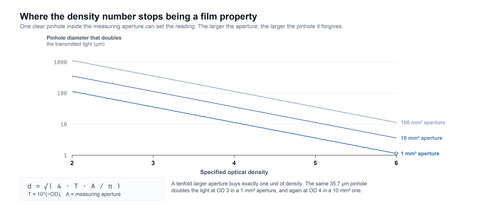
Put numbers on it. In a 1 mm² aperture, a single clear pinhole of 35.7 µm doubles the light at OD 3, 11.3 µm at OD 4, 3.6 µm at OD 5 and 1.1 µm at OD 6. None of those is a defect a visual inspection of the plate would single out, and none of them is a film property. Each is the size at which the measurement you chose stops being able to tell you the density of the film.
This is why a density figure without an aperture is not a requirement. If the drawing says OD 5 and the certificate was taken through a 1 mm² spot, the reading is a statement about a 1 mm² area that happened to be free of pinholes. If your incoming check uses a 10 mm² spot, your reading is expected to be lower for reasons that have nothing to do with the film. The published method on the product pages is worth quoting exactly here: optical properties are measured on one witness sample per lot, with density by densitometry, reflectance by spectrophotometry and film thickness by step profilometry. A witness-sample reading describes the run, not the plate in your hand.
What the film table can and cannot tell you
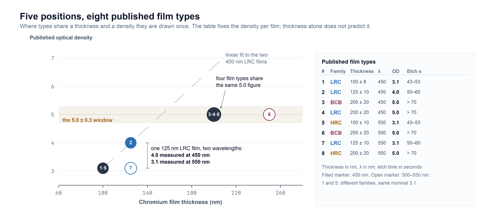
A density requirement has to land on a film that exists. The chrome-coated blank pages publish eight film types with thickness, density, the wavelength at which the density was taken, reflectance and wet-etch time. Put them on one chart and three things become visible that are hard to see in a table.
| Type | Family | Thickness | λ | Density | Wet etch | Density per nm |
|---|---|---|---|---|---|---|
| 1 | LRC | 100 ± 8 nm | 450 nm | 3.1 ± 0.2 | 43–53 s | 0.031 |
| 2 | LRC | 125 ± 10 nm | 450 nm | 4.0 ± 0.2 | 50–60 s | 0.032 |
| 3 | BCB | 200 ± 20 nm | 450 nm | 5.0 ± 0.3 | > 70 s | 0.025 |
| 4 | LRC | 200 ± 20 nm | 450 nm | 5.0 ± 0.3 | > 70 s | 0.025 |
| 5 | HRC | 100 ± 10 nm | 550 nm | 3.1 ± 0.2 | 43–53 s | 0.031 |
| 6 | BCB | 250 ± 20 nm | 500 nm | 5.0 ± 0.3 | > 70 s | 0.020 |
| 7 | LRC | 125 ± 10 nm | 550 nm | 3.1 ± 0.2 | 50–60 s | 0.025 |
| 8 | HRC | 200 ± 20 nm | 550 nm | 5.0 ± 0.3 | > 70 s | 0.025 |
Types 2 and 7 are both 125 nm of low-reflective chromium. One is measured at 450 nm and reads 4.0; the other is measured at 550 nm and reads 3.1. Nothing changed except the wavelength at which the question was asked. A straight-line interpolation would cost you 0.009 of density per nanometre of wavelength, which is enough to make a 450 nm reading a poor guide to a 436 nm exposure — and no guide at all to 365 nm.
Types 3, 4, 6 and 8 sit at 5.0 ± 0.3 across two thicknesses, three measurement wavelengths and three coating families. Meanwhile a linear absorption model fitted to the two 450 nm low-reflective films predicts 6.2 to 6.4 for a 200 nm film of that family, and the table publishes 5.0 for exactly that film. Read together, these two observations say something practical: the published density is a target set per film type, not a value that follows from thickness.
Etch time rises with thickness in the same table: 43–53 s for the 100 nm films, 50–60 s for 125 nm, and more than 70 s for the 200 nm and 250 nm ones. The published lateral-undercut designation for the 100 nm low-reflective coating is under 0.07 µm per 10 s, which puts 43–53 s at 0.30–0.37 µm per edge, and more than 70 s at over 0.49 µm per edge. The step from OD 3.1 to OD 5 therefore costs something in the region of 0.12 to 0.19 µm of undercut per edge.
What to write on the drawing
Four fields make the figure unambiguous, and four more say what it leaves out. The first group is the one that most often goes missing.
Make the number unambiguous
- Target density with its tolerance, and the words minimum, nominal or maximum
- The wavelength, in nm — the exposure wavelength, or the inspection wavelength if that is what the figure is for
- The measurement aperture, in mm² or as a diameter
- The reading method: narrowband densitometer or spectrophotometer band
State what the figure excludes
- Whether the reading is on a witness sample or on the part, and at how many positions
- Reflectance, if the film side matters to your alignment or inspection optics
- Pinholes and film defects, with their own acceptance rule
- Edge condition, cleaning and the usable area over which all of it applies
A generic entry such as "optical density: to specification" is what the product page currently offers, and it is an honest entry: the number genuinely depends on the application. But it moves the whole decision to the enquiry. If you can send those eight fields with a drawing, the density stops being a negotiation and becomes a check.
Inspection and acceptance
Density and defect acceptance are two different tests with two different sample sizes, and conflating them is the most common way a good plate gets rejected. Density is a lot-level optical check on a witness sample. Pinholes and film defects are a per-plate inspection over the usable area, against the limits agreed for that part. A plate can pass the first and fail the second, and no density figure — however high — will predict the second.
Where a standard or a customer quality agreement defines the acceptance method, that document governs, including the sampling plan and the pass thresholds. TL OPTIK does not publish a default pinhole count, a default aperture or a default sampling rate, and this guide does not create one. What can be agreed in writing is the method: the aperture, the wavelength, the instrument class, the number and position of readings, and the defect limits inside the usable area.
On acceptance figures. Density requirements are confirmed against the drawing, the purchase order and the agreed inspection method. Any numeric limit in this guide is either a published value or arithmetic on one; nothing here is a quality guarantee for an unquoted part.
Questions that come up before an order
Is OD 3 enough for a photomask?
For the exposure itself, almost always. OD 3 is 0.1 % transmission, which clears a leakage budget of K ÷ f up to 1000 — a 10× overexposure with 1 % of the clearing dose leaking through, or a 3× overexposure with 0.3 %. The published 3.1 film adds a little margin on top. What OD 3 does not do is guarantee anything about pinholes, and it says nothing about how the plate will look in a system with a bright illuminator. Those are separate requirements and should be written separately.
Should I specify OD 3 or OD 5?
Specify the lower one that satisfies a named mechanism, and name the mechanism. If the driver is resist clearing, Table 2 shows OD 3 is already one to two orders above the requirement. If the driver is stray light in a projection system, OD 5 may be justified — but it is a system requirement expressed as a plate number, and it should be discussed as one. A density figure with no stated wavelength, aperture and method is harder to meet than a lower figure with all three.
Does a thicker chromium film always give a higher density?
Within one coating family at one wavelength, yes — the two 450 nm low-reflective films go from 3.1 at 100 nm to 4.0 at 125 nm. Across families and wavelengths, no: a 100 nm high-reflective film reads 3.1 at 550 nm while a 200 nm blue-chrome film reads 5.0 at 450 nm, and the same 125 nm low-reflective film reads 4.0 at 450 nm but 3.1 at 550 nm. Thickness is one input to three.
Why does my densitometer read lower than the certificate?
Two usual causes, both worth checking before the plate is blamed. First, aperture: a larger measuring spot averages over more area, so pinholes and thin spots pull the reading down. Second, spectral response: a broadband densitometer weights the spectrum differently from a narrowband reading at a stated wavelength, and chrome density is strongly wavelength dependent — 0.9 between 450 and 550 nm on one film. Agree the aperture and the instrument class in writing, and the two readings should converge.
Can I order OD 6?
The published table runs to 5.0 ± 0.3 across four film types, so 6.0 is not a catalogue figure. Before asking for it, consider what it would mean to measure: at OD 6 in a 1 mm² aperture, a single 1.1 µm clear pinhole doubles the transmitted light. A requirement at that level is a requirement on defect density as much as on film, and both have to be agreed together. If the real need is lower leakage at a specific wavelength, say so — that can often be met by the film choice and confirmed by a reading at that wavelength.
Does optical density tell me how opaque the mask looks?
No. Density is transmission-only. Reflectance is a separate figure with a separate measurement: about 11 % at 436 nm for the low-reflective films, 7 % or less for the blue-chrome films at 600 nm, and 45 % or more for the high-reflective films. A film can be visually dark and still return enough light to disturb an alignment camera, which is why the two numbers appear in the same table and should appear on the same drawing.
Send the drawing, not the adjective
If you have a density figure and a reason for it, send both — with the wavelength and the measuring aperture. We will confirm which film in the published range reaches it, what the etch step does to the artwork bias, and how the reading will be taken. If the figure came from a specification written for a different process, that is worth settling before the plate is coated.