
How close can a pattern go to the cut edge of a glass part?
Not one number. Six widths sit between the artwork and the outline, at three different scales, and the one that binds your part is usually not the one you were worried about.
The short answer
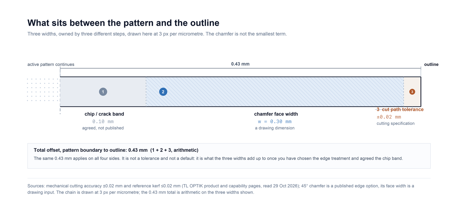
On a part cut from a larger plate, the minimum offset from the pattern boundary to the outline is the chamfer face width plus the outline tolerance plus half the kerf plus the chip band you are prepared to exclude. With a 45° chamfer of 0.30 mm on a 1.6 mm plate that comes to about 0.43 mm — and the chamfer, not the cutting accuracy, is normally the largest term.
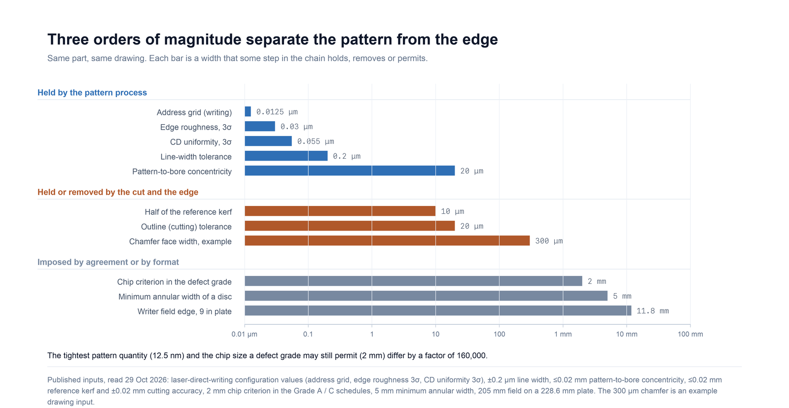
On a plate that fills the writing field, the field is the binding limit: a 205 mm field on a 228.6 mm (9 in) plate leaves 11.8 mm per side that no pattern can occupy at all.
The cut edge is not a usable datum for the pattern. TL OPTIK publishes ±0.2 µm for line width and ±0.02 mm for mechanical cutting. That is a factor of 100. Dimension the pattern from a machined feature or a common drawing origin, and state the edge distance as a minimum clearance rather than as a position tolerance.
The 0.43 mm above is a worked example, not a catalogue value. It is built from published limits and one drawing input; the inputs are listed where each term is introduced.
Most of the confusion around this question comes from treating the edge as a line. It is not. Between the last feature of the artwork and the outside of the part there is a zone that several different steps each claim a slice of, and each slice is specified in a different document: the writer's field, the cutting tolerance, the kerf, the chamfer, the chip band, the coating area, and the land your fixture clamps on.
Six widths, three scales
The table below is the whole model. Two of the six are measured in micrometres, one in tenths of a millimetre, one in millimetres, and two are not widths at all in the ordinary sense but areas that carry no guarantee.
| Item | Published or agreed value | What it does to the pattern |
|---|---|---|
| Writing field edge | 205 × 205 mm or 410 × 410 mm | On a full-format plate, the last few millimetres cannot be written at all. Set by the writer, not by the glass. |
| Outline tolerance | ±0.02 mm | The cut edge can land anywhere inside this band on any side, so the gap you get is the gap you asked for, ±0.02 mm. |
| Kerf | Reference ≤0.02 mm | Material removed by the cut itself. Half of it is consumed on the pattern side of the programmed path. |
| Chamfer | 45°, face width from the drawing | Removes a strip of the polished face along every edge. Usually the largest single term. |
| Chip and crack band | Agreed; the grade only forbids chips above 2 mm | The zone next to the cut where you will not accept an interruption. If you do not define it, the acceptance criterion decides it for you. |
| Coating, resist and fixture | ±1% uniformity over the agreed area; edge-bead exclusion; clamp land | Outside the agreed measurement area there is no stated uniformity, and under a clamp there is no usable optical surface. |
Three of these are genuinely dimensional losses: outline tolerance, kerf and chamfer. They add up directly and they are the ones a designer can calculate. The other three are conditions: the writer cannot reach there, the coating is not specified there, the fixture covers it. A drawing that states one number for "edge distance" is silently blending all six.
Why the cut edge cannot be the pattern datum
It is tempting to dimension a pattern as "0.5 mm from the edge". That works only while the edge stays where you think it is, and the numbers say it does not. TL OPTIK publishes three quite different classes of geometric requirement, and they differ by two orders of magnitude.
| Class | Published value | What it measures | Can the pattern be dimensioned from it? |
|---|---|---|---|
| Feature size | ±0.2 µm | Width of one line, at an agreed edge threshold | Not applicable — this is a size, not a position |
| Pattern to a machined feature | ≤0.02 mm | Position of the pattern relative to a bore or a specified centre | Yes — this is the relation to use |
| Cut outline | ±0.02 mm | Where the cut edge lands relative to the programmed path | No — 100× coarser than the line width |
| Edge condition | 0.015 in/in | How far the edge at one face sits from the edge at the other, per unit thickness | No — the reference moves with thickness |
The gap between the first two rows and the third is the point. A line is placed to two-tenths of a micrometre; the outline it sits near is placed to twenty micrometres. Dimensioning the pattern from the outline is like dimensioning a machined bore from a sawn end — the number is not wrong, it just describes a different object. TL OPTIK's own cutting page makes the same distinction in one line: outline dimensions and pattern-to-bore position are separate requirements, and the specified positional relationship has to be inspected against a common datum.
So the drawing needs two separate statements, not one. First, where the pattern sits, expressed against a datum that survives cutting: a bore, a machined reference edge, or the coordinate origin shared by the artwork and the cut file. Second, how much material must remain between the outermost feature and the outline, expressed as a minimum. The first is a position; the second is a clearance. Mixing them produces a drawing that a supplier can satisfy and an inspector cannot verify.
What the cut itself takes
Two numbers are usually quoted as if they were one. They are not.
- Outline tolerance describes where the finished edge lands relative to the programmed path. TL OPTIK publishes ±0.02 mm mechanical cutting accuracy on its encoder-disc and scale pages. It is a position error: the whole edge can move, and it can move by a different amount on the opposite side.
- Kerf describes how much material the cut removes. The UV laser cutting page gives a reference kerf width of ≤0.02 mm and notes that cutting depth and width are controlled by process parameters. Kerf is a width, not an error.
For an edge budget the two enter differently. The kerf only matters as half its width, because the programmed path is normally the finished outline and the cut removes 0.01 mm to either side of it. The outline tolerance enters at full value, because it moves the edge bodily. Together they are 0.02 + 0.01 = 0.03 mm — about 7% of the 0.43 mm example, and rarely the term that decides the design.
The ±0.02 mm figure is published as a mechanical cutting accuracy for encoder discs, scales and patterned glass outlines. It is a tolerance class for a cut profile, not a promise about any particular part. A part with a 3 mm wall, a sharp internal corner or a 0.4 mm thickness may behave differently, and the drawing should say which profile the tolerance applies to.
What the edge treatment takes
A ground edge is not a square corner. TL OPTIK lists a 45° chamfer as the edge preparation option on its precision-substrate tables, and the chamfer consumes face width on every side. If the face width is w, the usable polished face is the outline minus 2w in each direction. The width is a drawing dimension: the published order pages state the chamfer angle, not a default width, so w has to come from your drawing or from the quotation.
A second, less obvious term is the lean of the cut face. TL OPTIK specifies edge squareness two ways: a linear option of <0.015 in per 1 in of reference length, and a separate blank-edge specification of 90° ±5′. The first is a ratio — 0.015, or about 0.86°. The second is an angle — 5 arc minutes, or 0.00145 as a ratio. Over the same thickness, the linear option permits roughly ten times the lean.
Why it matters: the edge you measure on the top face is not the edge on the bottom face. For a plate of thickness t, the lateral offset is δ = s × t, where s is the squareness ratio. On a 1.6 mm plate the linear option allows 24 µm; on a 12 mm plate it allows 180 µm, which is most of a 0.2 mm gap.
| Plate thickness | Lean, <0.015 in/1 in | Lean, 90° ±5′ |
|---|---|---|
| 0.3 mm | 4.5 µm | 0.44 µm |
| 1.0 mm | 15 µm | 1.5 µm |
| 1.6 mm | 24 µm | 2.3 µm |
| 3.0 mm | 45 µm | 4.4 µm |
| 6.0 mm | 90 µm | 8.7 µm |
| 12 mm | 180 µm | 17.5 µm |
All six values are arithmetic on the two published ratios. They describe a geometric allowance, not a measured lean on any supplied part.
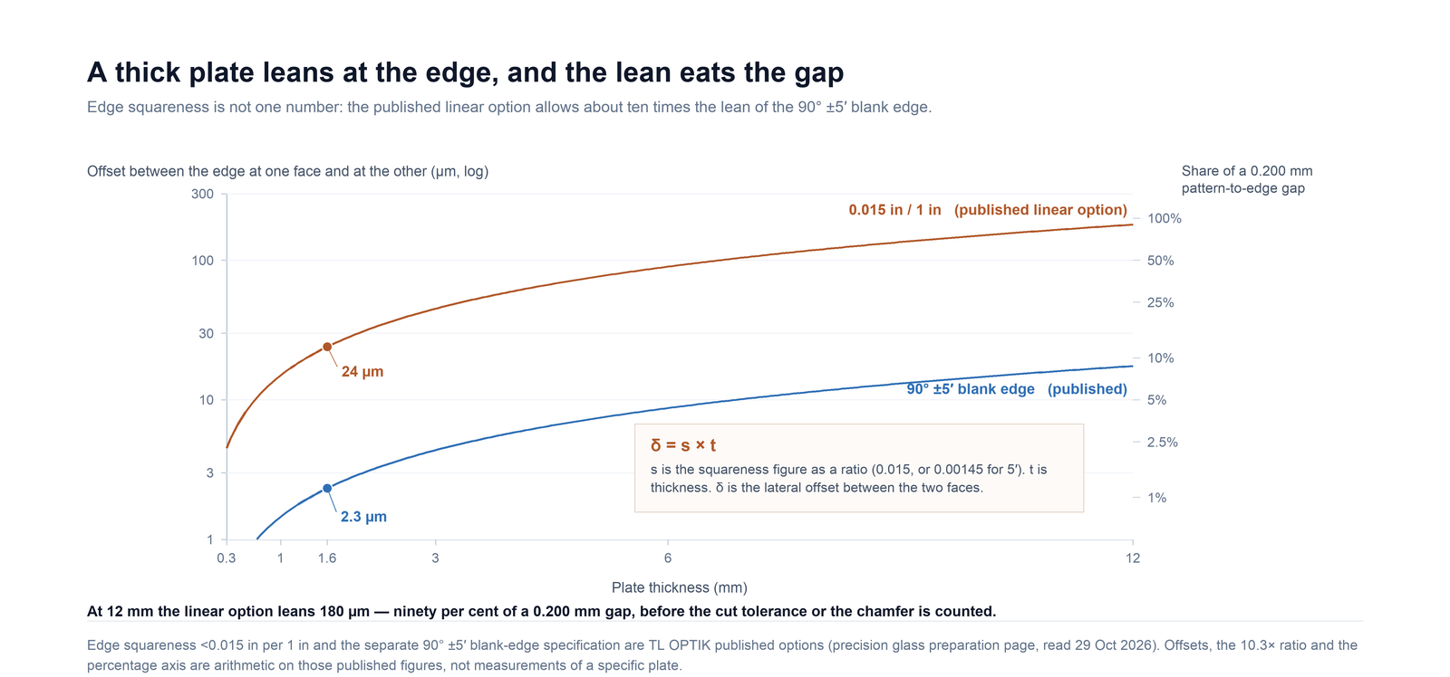
The practical consequence: on thin plates the lean is irrelevant next to the chamfer. On plates above roughly 3 mm it becomes a term you have to add, and above 6 mm it is worth asking which squareness specification the quotation is based on — the two published options differ by a factor of ten and both are legitimate.
What the chip band costs, and why the grade will not settle it
Cutting leaves a damaged zone along the edge: micro-cracks, occasional chips, sometimes a burr. The published substrate defect schedules treat this coarsely. Both the Grade A and the Grade C schedules forbid cracks and chips above 2 mm; neither sets a limit for a 0.3 mm chip. The section instead ends with an instruction: counts refer to defects in the agreed inspection area, and the usable area and excluded edges must be defined on the drawing.
That is an honest arrangement, but it pushes a decision onto the buyer. A 2 mm chip criterion is 100 times the cutting tolerance and nearly seven times the chamfer in the example above. If your pattern sits 0.5 mm from the outline and your acceptance document only quotes the grade, a 1.9 mm chip in that band is not excluded by anything. Three ways out, in order of preference:
- Define the band and forbid interruptions inside it. "No chips or cracks within 0.10 mm of the outline" is a clear, inspectable clause. It is stricter than the grade and it is the only version that actually protects a pattern placed close to the edge.
- Widen the band to 2 mm and accept the area loss. Consistent with the published schedule, but expensive on small parts (see the next section).
- Separate the zones. Allow chips in a handling border and forbid them in the functional area. This is what the encoder-disc and inspection guidance already asks for: active tracks, clamp areas and edge exclusion zones identified separately on the DWG.
What the coating, the resist and the fixture take
Three more exclusions are not about the glass at all.
Coating. TL OPTIK targets ±1% film uniformity over the agreed measurement area. The phrase carries the whole constraint: outside that area there is no stated uniformity, and the edge of a sputtered or sprayed plate is normally outside it. If a pattern needs uniform optical density to within a few percent right up to the cut edge, the measurement area has to be agreed to include that strip, or the design has to accept the gradient.
Resist. A spin-coated plate has an edge bead. TL OPTIK lists edge-bead exclusion as part of the coated-plate order alongside resist model, thickness and coated area — it is a specified quantity, not a defect. A pattern written into the bead region inherits whatever thickness profile the bead has.
The fixture. A retaining ring, an adhesive bead or an O-ring needs a land, and the land is not optically usable. The same is true of a vacuum chuck that pulls the plate flat: the area under the seal is mechanically useful and optically dead. On a 79 mm encoder disc with a 51 mm bore, the ring is 14 mm wide; a hub clamp of 3 mm and a 0.3 mm chamfer at each edge leave about 10.4 mm for the tracks before any readhead clearance is considered.
A worked example: 25 mm part, 1.6 mm soda-lime, 45° chamfer
The inputs, stated so you can substitute your own: outline tolerance 0.02 mm, kerf 0.02 mm (half consumed, 0.01 mm), chamfer face width 0.30 mm, chip band 0.10 mm agreed with the supplier.
0.30 + 0.02 + 0.01 + 0.10 = 0.43 mm
The usable face is then 25 − 0.86 = 24.14 mm square, which is 93.2% of the area — a loss of 6.8%. The same 0.43 mm band on a 228.6 mm plate costs 0.75%. Nothing about the band changed; only the part got bigger.
| Plate side | 0.08 mm | 0.43 mm | 2.0 mm |
|---|---|---|---|
| 10 mm | 3.2% | 16.5% | 64% |
| 25 mm | 1.3% | 6.8% | 29% |
| 50 mm | 0.64% | 3.4% | 15% |
| 100 mm | 0.32% | 1.7% | 7.8% |
| 228.6 mm | 0.14% | 0.75% | 3.5% |
| 431.8 mm | 0.07% | 0.40% | 1.8% |
Two readings follow. First, on a 10 mm part an edge band is a design decision with real area consequences, not a rounding error — a 2 mm handling border removes almost two thirds of the face. Second, the argument for a wide border on a large plate is weak on area grounds and strong on handling grounds; those are different reasons, and the drawing should say which one applies.
Now the comparison that matters commercially. Drop the chamfer and specify a plain ground edge with a 0.05 mm chip band instead: the offset becomes 0.02 + 0.01 + 0.05 = 0.08 mm, and the same 25 mm part loses 1.3% instead of 6.8%. Choosing a 45° chamfer therefore costs about 5.5 percentage points of face area on a part this size. That is a fair price for a protected edge on a handled part, and a poor one on a part that is bonded into a housing and never touched.
Three part types, three different answers
The same question has three answers because the binding term changes with the part.
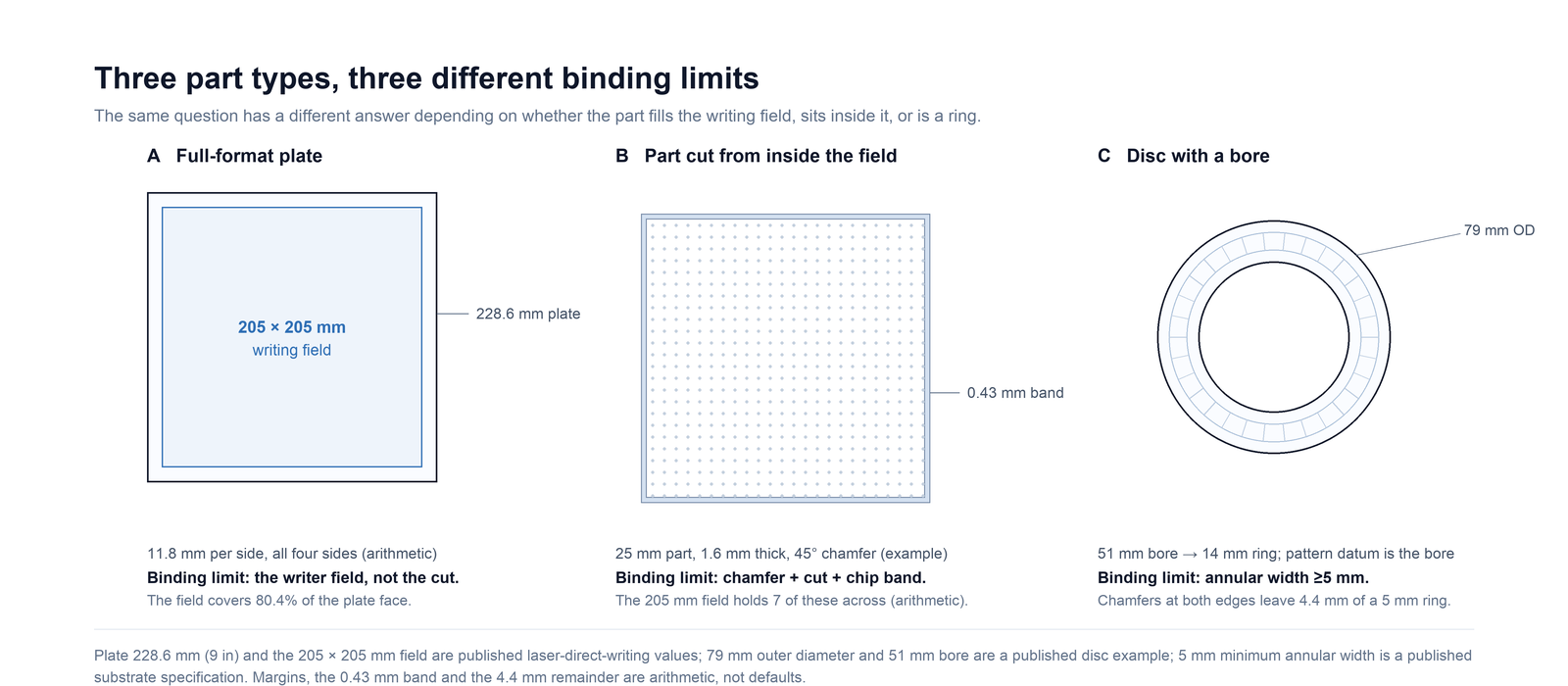
| Part type | Binding width | What the drawing must state |
|---|---|---|
| Full-format plate | The writing field: 11.8 mm per side on 9 in, 10.9 mm on 17 in | Whether the artwork may be stitched across fields, and where a seam is acceptable |
| Part cut from inside the field | Chamfer plus cut plus chip band: 0.43 mm in the example | The minimum clearance, the chamfer width, and whether chips are permitted in the band |
| Disc or ring | Annular width, minimum 5 mm, minus chamfers and clamp land | Bore as datum, track radii, clamp land, and the pattern-to-bore position (≤0.02 mm) |
The ring case deserves its own line
On a disc, the edge question arrives from both sides at once. TL OPTIK specifies a minimum annular width of 5 mm for encoder glass substrates, and a maximum disc diameter of 1500 mm with ≤0.02 mm pattern-to-bore concentricity. A 5 mm ring is the narrowest the substrate specification allows; put a 0.3 mm chamfer on the outside and the inside and 4.4 mm of it remains. If the readhead also needs a clear annulus, the tracks may not fit — and the answer is a larger diameter or a closed disc, not a narrower ring.
Because the bore is the datum, the ring case is also the one where the pattern position is properly specified. A 79 mm disc with a 51 mm bore and a track at 32 mm radius is dimensioned from the bore centre, and the outside diameter only has to clear the housing. That is the model to copy on a rectangular part: find the machined feature, dimension from it, and let the outline carry a clearance instead of a position.
What to put on the drawing
The list below is what a supplier needs in order to quote an edge margin rather than guess one. It is not a template for every part — a part with no cut edge needs none of it — but each line corresponds to one of the widths in the model, and omitting it moves the decision to the supplier.
| Item | What to state | Why it changes the answer |
|---|---|---|
| Active pattern boundary | A closed boundary for the functional area, distinct from the artwork extents | Defines what the offset is measured from; a stray alignment mark outside the boundary should not consume the band |
| Datum | Bore, machined edge or shared origin, with the pattern position tolerance against it | The only datum that survives cutting; replaces "0.5 mm from the edge" |
| Minimum clearance | A single minimum value from boundary to outline, with a note that it applies on all sides | Turns the edge distance into a clearance the supplier can hold without knowing your datum intent |
| Edge preparation | Chamfer angle and face width, or "ground edge, no chamfer" | The chamfer is the largest single term; leaving the width open makes the quote ambiguous |
| Cut profile | Which edges are cut, which are ground, and the narrowest wall between features | Kerf and outline tolerance behave differently on a thin wall than on a long straight edge |
| Chip criterion in the band | Permitted or forbidden, with size if permitted | The published grade only forbids chips above 2 mm; anything smaller needs your clause |
| Coating area | The area over which uniformity and optical density are required | Uniformity is specified over an agreed area, and the edge is normally outside it |
| Clamp or bond land | Where the fixture contacts the part, and whether that area may carry pattern | A land is mechanically necessary and optically dead; if it overlaps the pattern, the part is scrap |
| Inspection area | The area over which the defect schedule is applied, with the excluded border dimensioned | The schedules count defects in an agreed area, and the excluded edges must be drawn |
How the band is checked
An edge margin is easy to specify and easy to check badly. Three points are worth agreeing before the first part:
- Which face. On a chamfered plate the top face and the bottom face have different outlines. The clearance should name the face, or the datum face, not "the edge".
- How the edge position is measured. A profile projector, a measuring microscope and a vision system will agree to within a few micrometres on a straight ground edge and disagree on a laser-cut edge with a visible kerf slope. The measurement method belongs in the acceptance document.
- What is being reported. A minimum clearance measured at one point does not demonstrate the clearance around the part. If the requirement is "at least 0.43 mm on all sides", the record needs the minimum of a set of positions, and the positions need to be named.
None of this replaces the agreed drawing. Final acceptance follows the drawing revision, the purchase order and any quality agreement, and the inspection record has to reference them. The suggestions above describe how to write a requirement that can be inspected — they are not a tolerance the supplier has already agreed to, and they are not a quality guarantee for an unquoted part.
Common questions
Can I put a pattern 0.10 mm from a laser-cut edge?
Only with a plain edge and a narrow chip band. The cut tolerance (0.02 mm) and half the kerf (0.01 mm) already use 0.03 mm of it, leaving 0.07 mm for chamfer and chip band together — which rules out a 45° chamfer of any practical width. At that distance the edge also has to be excluded from the defect criteria by an explicit clause, because the published grade permits chips up to 2 mm in the inspection area.
Is the cutting tolerance the same thing as the kerf?
No. Kerf is the width of material the cut removes — a reference value of ≤0.02 mm on the UV laser cutting route. Cutting accuracy is where the finished edge lands relative to the programmed path, published as ±0.02 mm. In an edge budget the kerf contributes half its width and the accuracy contributes its full value.
Which datum should the pattern use if the part has no bore?
A machined edge or a common drawing origin shared by the artwork and the cut file. A ground edge is a far better reference than a cut edge because its position is set by a different process. If neither exists, place the pattern relative to fiducials that are themselves patterned, and state the relationship between the fiducials and the outline as a separate requirement.
Does the chamfer have to be on both faces?
That is a drawing decision, and it changes the area more than people expect. Each chamfered face loses the face width on every side. A single-face chamfer halves the loss on the plain face and leaves one edge sharp — which may be acceptable in a housing and unacceptable on a handled part.
How do I stop a 1 mm chip from being accepted at the edge?
Write it into the drawing. Both published substrate grades forbid cracks and chips only above 2 mm, and both tell the buyer to define the usable area and the excluded edges. A clause such as "no chips or cracks within 0.10 mm of the outline, regardless of size" is stricter than the grade and is the only form that protects a pattern placed close to the edge.
Do I need the full 410 mm field?
Only if the part fills the plate. The writing field is 205 × 205 mm or 410 × 410 mm, against maximum substrate formats of 9 × 9 in and 17 × 17 in. A 9 in plate leaves 11.8 mm per side that the field cannot reach in one exposure; anything smaller than the field has no field margin at all, and the cut and the chamfer become the only edge terms.
Send the drawing and the edge requirement together
A quotation for a patterned part is only as good as the edge definition behind it. Include the outline, thickness and material grade; the datum feature and its position tolerance; the minimum clearance; the edge preparation; the cut profile; and the chip criterion inside the band.